Opens in a new tab

Home » Integrated Circuits ICs » SN74LVC16244ADGGR

SN74LVC16244ADGGR

16-bit non-inverting buffer/driver, 3-state outputs, 1.65-3.6V, 48-TSSOP

8693

Effective Inventory

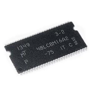
Image for reference only

Manufacturer Part:

SN74LVC16244ADGGR

Package:

TSSOP-48 (12.5 x 8.1 x 1.05 mm)

Brand:

Product Categories:

Quality Commitment

Shipping & Payment

Service & Packaging

Product Manual

Other recommendations you may be interested in.

Description

Product Overview

The SN74LVC16244ADGGR from Texas Instruments is a 16-bit buffer/driver with 3-state outputs, designed for 1.65-V to 3.6-V VCC operation. Packaged in a 48-pin TSSOP, it is a member of the TI Widebus family optimized for high-performance memory address driving, clock driving, and bus-oriented signal routing. The device can be configured as four 4-bit buffers, two 8-bit buffers, or one 16-bit buffer.

Key Specifications

Supply Voltage 1.65 V to 3.6 V
Number of Channels 16
Output Type 3-State
Output Drive (IOL/IOH) +-24 mA at 3.3 V
Max Propagation Delay 4.1 ns at 3.3 V
Operating Temperature -40 to 125 degC
Package 48-TSSOP (12.5 x 8.1 mm)

Features

  • 5-V tolerant inputs accepting voltages to 5.5 V
  • Ioff supports partial-power-down mode operation
  • Supports mixed-mode signal operation (5-V I/O with 3.3-V VCC)
  • Low typical VOLP (ground bounce) less than 0.8 V at 3.3 V
  • Latch-up performance exceeds 250 mA per JESD 17
  • ESD protection exceeds JESD 22 (2000-V HBM, 1000-V CDM)

Applications

  • Memory address drivers
  • Clock drivers and buffer arrays
  • Bus-oriented receivers and transmitters
  • 3.3-V to 5-V logic level translation
  • Server and networking equipment
Product Introduction: SN74LVC16244ADGGR Product Introduction

The SN74LVC16244ADGGR is a 16-bit buffer/driver with 3-state outputs from Texas Instruments, designed for 1.65-V to 3.6-V VCC operation. As a member of the TI Widebus family, it is specifically optimized for high-performance 3-state memory address drivers, clock drivers, and bus-oriented receivers and transmitters. The device can be flexibly configured as four 4-bit buffers, two 8-bit buffers, or one 16-bit buffer, providing true data outputs with symmetrical active-low output-enable (OE) inputs. Inputs accept voltages up to 5.5 V, enabling use as a logic translator in mixed 3.3-V and 5-V system environments.

Working Principle: SN74LVC16244ADGGR Working Principle

The SN74LVC16244ADGGR consists of four independent 4-bit buffer sections, each controlled by an active-low output-enable (1OE, 2OE, 3OE, 4OE) input. When the OE input is low, the corresponding buffer section passes data from input to output with true polarity. When OE is high, the outputs assume a high-impedance state, allowing bus sharing. The Ioff circuitry ensures that when VCC is zero, the outputs are disabled, preventing damaging backflow current through the device. The 5-V tolerant inputs use an input structure that can safely accept voltage levels above VCC, enabling mixed-voltage system interfacing.

Pin Description: SN74LVC16244ADGGR Pin Definition and Functions
Pin Name Type Function
1 1OE Input Output enable 1 (active low)
2-5 1A0-1A3 Input Data inputs section 1
7-10 1Y0-1Y3 Output Data outputs section 1
13 2OE Input Output enable 2 (active low)
14-17 2A0-2A3 Input Data inputs section 2
19-22 2Y0-2Y3 Output Data outputs section 2
25 GND Power Ground
24 3OE Input Output enable 3 (active low)
26-29 3A0-3A3 Input Data inputs section 3
30-33 3Y0-3Y3 Output Data outputs section 3
36 4OE Input Output enable 4 (active low)
37-40 4A0-4A3 Input Data inputs section 4
41-44 4Y0-4Y3 Output Data outputs section 4
48 VCC Power Supply voltage
Application Scenarios: In which products and applications is SN74LVC16244ADGGR used
  • Memory address bus drivers in servers and workstations
  • Clock distribution and buffering networks
  • 3.3-V to 5-V logic level translation in mixed-voltage systems
  • Backplane bus drivers in telecommunications equipment
  • Industrial control system signal buffering
Alternative Models: What chips are recommended as replacements for SN74LVC16244ADGGR
Manufacturer Part Number Package Notes
TI SN74LVC16244ADLR SSOP-48 Same function, different package
Nexperia 74LVC16244ADGG TSSOP-48 Pin-compatible equivalent
TI SN74LVCH16244ADGGR TSSOP-48 With bus-hold on inputs
Nexperia 74LVCH16244ADGG TSSOP-48 Bus-hold variant
TI SN74ALVC16244ADGGR TSSOP-48 ALVC family, higher speed

Recommend Parts

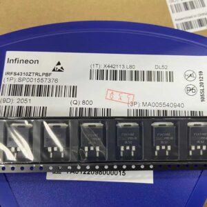
IRFS4310ZTRLPBF

IRFS4310ZTRLPBF – 100V N-Channel HEXFET Power MOSFET, 7 mΩ RDS(on), D2PAK (TO-263AB)

Brand: infineon

Package: D2PAK (TO-263AB)

IN STOCK: 11137pcs

Cargo cycle: 3-7 Days

The minimum order is 1

MSASJ105BB5475MFNA01

4.7uF 6.3V X5R MLCC, 0402, Taiyo Yuden

Brand: gigadevice

Package: 0402 (1005 Metric, 1.0 x 0.5 x 0.5 mm)

IN STOCK: 9701pcs

Cargo cycle: 3-7 Days

The minimum order is 1

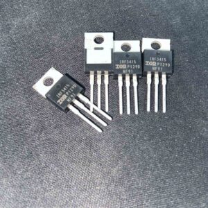
IRF3415PBF

150V N-channel power MOSFET, 43A, 41mΩ RDS(on), TO-220AB package

Brand: infineon

Package: TO-220AB

IN STOCK: 2940pcs

Cargo cycle: 3-7 Days

The minimum order is 1

105017-1001

USB Type-C receptacle connector, 24-pin, SMD

Brand: Amphenol

Package: SMD (8.9 x 7.3 x 3.2 mm, right angle)

IN STOCK: 5335pcs

Cargo cycle: 3-7 Days

The minimum order is 1

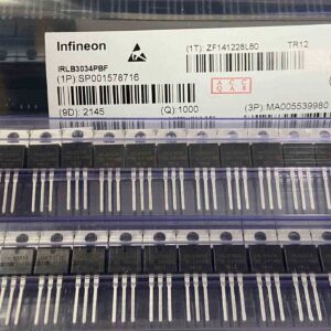
IRLB3034PBF

IRLB3034PBF – 40V N-Channel StrongIRFET Power MOSFET (Logic Level), 1.7 mΩ (max) @ 10V; 2.0 mΩ @ 4.5V RDS(on), TO-220AB

Brand: infineon

Package: TO-220AB

IN STOCK: 9724pcs

Cargo cycle: 3-7 Days

The minimum order is 1

XC6SLX75-2FGG484I

Spartan-6 LX75 FPGA, 74637 logic cells, 132 DSP, 3096KB BRAM, 408 I/O, FBGA-484 23x23mm, -2 speed, industrial -40~100C, AMD Xilinx

Brand: xilinx

Package: FGG484 (484-ball fine-pitch BGA, 23x23mm body, 1.0mm ball pitch, 22×22 ball array, 6 I/O banks, lead-free)

IN STOCK: 890pcs

Cargo cycle: 3-7 Days

The minimum order is 1