Opens in a new tab

Home » Integrated Circuits ICs, Memory » MX60UF8G18AC-XKI

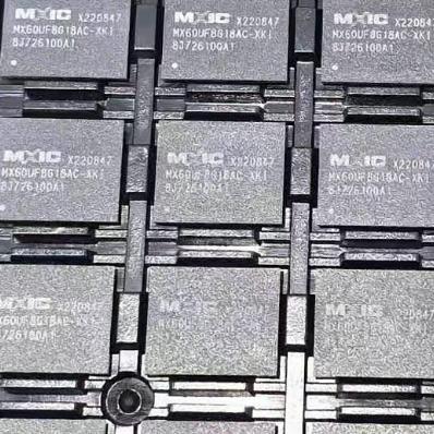
MX60UF8G18AC-XKI

1.8V 8Gb SLC NAND Flash, ONFI 1.0, 2K+64B page, 100K P/E cycles, 63-VFBGA 9x11mm Industrial

5634

Effective Inventory

Image for reference only

Manufacturer Part:

MX60UF8G18AC-XKI

Package:

63-VFBGA (9mm x 11mm, 0.8mm pitch)

Brand:

Product Categories:

Quality Commitment

Shipping & Payment

Service & Packaging

Product Manual

Description

Product Overview

The MX60UF8G18AC-XKI is a 1.8V, 8Gb SLC (Single-Level Cell) NAND Flash Memory device from Macronix (MXIC), belonging to the MX60UF 1.8V family. It is stacked from two 4Gb die, each organized with two planes of 2048 blocks. The device features a (2048+64)-byte page size, (128K+4K)-byte block size, ONFI 1.0 compliant interface, and supports Cache Read/Cache Program and Two-Plane operations. The -XKI suffix denotes the 63-VFBGA (9mm × 11mm) package with industrial-grade temperature range (-40°C to +85°C). With a typical P/E endurance of 100K cycles (with 4-bit ECC per 528 bytes), it is well-suited for embedded system code and data storage in mobile, M2M, and low-voltage applications.

Key Specifications

Manufacturer Macronix (MXIC)
Density 8Gb (1G × 8)
Cell Type SLC (Single-Level Cell)
Voltage (VCC) 1.7V – 1.95V
Bus Width x8
Interface Parallel, ONFI 1.0 Compliant
Page Size (2048 + 64) bytes
Block Size (128K + 4K) bytes = 64 pages per block
Plane Size 2 planes per die, 2048 blocks per plane
Die Stack 2 × 4Gb die (Multi-die)
ECC Requirement 4-bit ECC per (512+16) bytes
Random Read Access (tR) 25 μs (typ.)
Sequential Read Speed 25 ns per byte
Access Time 22 ns
Page Program Time 320 μs (typ.), 600 μs (max)
Block Erase Time 1 ms (typ.), 3.5 ms (max)
Active Current 30 mA (max)
Standby Current 100 μA (max)
Endurance 100,000 P/E cycles (typ.)
Data Retention 10 years
Operating Temperature -40°C to +85°C (Industrial)
Guaranteed Good Block Block #0 at shipping
Secure OTP Supported (30 pages)
Unique ID ONFI standard
Electronic Signature 5 cycles
Two-Plane Operations Supported
Chip Enable Don’t Care Supported
Package 63-VFBGA, 9mm × 11mm, 0.8mm ball pitch
RoHS / Halogen-Free Yes

Features

  • 8Gb SLC NAND Flash with high reliability (100K P/E cycles typical)
  • 1.8V low-voltage operation (1.7V – 1.95V) for mobile and M2M applications
  • Two 4Gb die stacked with interleaved die operation support
  • ONFI 1.0 compliant parallel interface with command/address/data multiplexing
  • Cache Read and Cache Program for improved throughput
  • Two-Plane Program and Two-Plane Cache Program support
  • Secure One-Time Programmable (OTP) area: 30 pages
  • Unique ID Read (ONFI standard) and Electronic Signature (5 cycles)
  • Hardware write protection via WP# pin
  • Chip Enable Don’t Care for simplified system interface
  • Low power: 30 mA active / 100 μA standby
  • Industrial temperature range: -40°C to +85°C

Applications

  • Mobile phones and 3G/4G/5G data cards requiring low-voltage NAND storage
  • M2M (Machine-to-Machine) devices and IoT edge nodes
  • Embedded system code and data storage in portable electronics
  • Industrial control systems with 1.8V logic
  • Boot code and configuration storage in low-power FPGA / SoC platforms
Product Introduction: MX60UF8G18AC-XKI Product Introduction

The MX60UF8G18AC-XKI is a 1.8V, 8Gb SLC NAND Flash Memory device from Macronix, belonging to the MX60UF 1.8V family designed for mobile and M2M embedded applications. It is stacked from two 4Gb die, each organized with two planes of 2048 blocks, where each block contains 64 pages of (2048+64) bytes. The device supports the ONFI 1.0 standard interface with command/address/data multiplexing on an 8-bit bus. Key features include Cache Read/Cache Program, Two-Plane operations, Secure OTP (30 pages), Unique ID Read (ONFI), and Electronic Signature (5 cycles). With a typical P/E endurance of 100K cycles (requiring 4-bit ECC per 528 bytes) and 10-year data retention, the MX60UF8G18AC-XKI is ideal for low-voltage embedded system code and data storage. The -XKI suffix denotes the 63-VFBGA (9x11mm) industrial-grade package.

Working Principle: MX60UF8G18AC-XKI Working Principle

The MX60UF8G18AC-XKI operates as a 1.8V parallel SLC NAND Flash memory with an ONFI 1.0 compliant interface. Commands, addresses, and data are multiplexed through the 8-bit I/O[7:0] bus, controlled by CLE (Command Latch Enable), ALE (Address Latch Enable), CE# (Chip Enable), WE# (Write Enable), RE# (Read Enable), and WP# (Write Protect) signals. Read operations: A Read command (00h-30h) initiates page transfer from the NAND array to the 2112-byte page buffer (tR = 25us typical), after which data is output sequentially at 25ns per byte on RE# falling edges. Cache Read allows overlapping array-to-buffer transfer of the next page while the current page is being output. Program operations: A Page Program command (80h-10h) loads data from I/O into the page buffer and programs the selected page (320us typical). Cache Program (80h-15h) allows pipelined programming. Two-Plane Program enables simultaneous programming of two pages on different planes. Erase operations: A Block Erase command (60h-D0h) erases a 128K+4K byte block in 1ms typical. The two stacked 4Gb die share a single CE# and R/B# signal (Mode A). The R/B# open-drain output indicates device busy/ready status.

Pin Description: MX60UF8G18AC-XKI Pin Definition and Functions
Ball Name Type Function
A3 WP# Input Write Protect (active low); low = block program/erase disable
A1, D1, G1, K1 VCC Power 1.7V – 1.95V supply voltage
A7, D7, G7, K7, M1 VSS Ground Ground connection
B7, C7, J7, L7 NC — Not connected internally
C6 CE# Input Chip Enable (active low); high = standby, low = active
D6 WE# Input Write Enable; address/data/command latched at WE# rising edge
E5 CLE Input Command Latch Enable; high = command on I/O at WE# rising
F5 ALE Input Address Latch Enable; high = address on I/O at WE# rising
F6 RE# Input Read Enable; data output tREA after RE# falling edge
G8 R/B# Output (OD) Ready/Busy status (open-drain); low = busy, high = ready
H7, H6, J5, J6, K5, L5, L6, M6 I/O[7:0] I/O Multiplexed command/address/data bus
H5 DNU — Do Not Use (do not connect)
Application Scenarios: In which products and applications is MX60UF8G18AC-XKI used
  • Mobile phone and 3G/4G/5G data card mass storage at 1.8V logic level
  • M2M (Machine-to-Machine) devices and IoT edge nodes requiring low-voltage NAND
  • Portable and wearable electronics embedded code and data storage
  • Industrial control systems with 1.8V rail and high reliability SLC endurance (100K P/E cycles)
  • Low-power FPGA / SoC boot media and configuration storage in battery-powered platforms
Alternative Models: What chips are recommended as replacements for MX60UF8G18AC-XKI
Manufacturer Part Number Package Notes
Macronix MX60UF8G28AD-XKI 63-VFBGA 8Gb 1.8V SLC, 4K page, 8-bit ECC, newer AD generation
Macronix MX60LF8G18AC 48-TSOP / 63-VFBGA 8Gb 3V SLC, 2K page, 4-bit ECC (3V version)
Macronix MX30UF4G18AB 48-TSOP / 63-VFBGA 4Gb 1.8V SLC, 2K page, 4-bit ECC, single-die
Winbond W25N01KV 8-SOIC / WSON 1Gb SLC SPI NAND alternative
Micron MT29F8G08AABAH4 48-TSOP 8Gb SLC NAND, 3V, ONFI 2.1

Recommend Parts

TMP275AIDR

0.5C I2C temp sensor, 12-bit, 2.7-5.5V, alert output, 8-SOIC

Brand: TI

Package: 8-SOIC (4.90 x 3.91 x 1.50 mm)

IN STOCK: 3681pcs

Cargo cycle: 3-7 Days

The minimum order is 1

IL41050TA-3E

NVE IL41050TA-3E IsoLoop isolated CAN transceiver, 2.5kVrms isolation, 1Mbps, 16-SOIC

Brand: nve

Package: SOIC-16 NB

IN STOCK: 3150pcs

Cargo cycle: 3-7 Days

The minimum order is 1

IRFS4115TRLPBF

IRFS4115TRLPBF – 150V N-Channel HEXFET Power MOSFET, 12.1 mΩ RDS(on), D2PAK (TO-263)

Brand: infineon

Package: D2PAK (TO-263)

IN STOCK: 6965pcs

Cargo cycle: 3-7 Days

The minimum order is 1

CD4070BM96

Quad 2-input XOR gate, 3-18V CMOS, 65ns at 10V, SOIC-14

Brand: TI

Package: SOIC-14 (8.75 x 3.9 x 1.5mm)

IN STOCK: 4245pcs

Cargo cycle: 3-7 Days

The minimum order is 1

MX29LV800CBTI-70G

8Mbit Parallel NOR Flash, Bottom Boot, 70ns, 2.7-3.6V, 48-TSOP

Brand: Macronix

Package: 48-TSOP

IN STOCK: 9345pcs

Cargo cycle: 3-7 Days

The minimum order is 1

LMC7101AIM5X/NOPB

Single CMOS RRIO op-amp, 1.4MHz, SOT-23-5

Brand: TI

Package: SOT-23-5 (2.9 x 1.6 x 1.1 mm)

IN STOCK: 11389pcs

Cargo cycle: 3-7 Days

The minimum order is 1