


Opens in a new tab

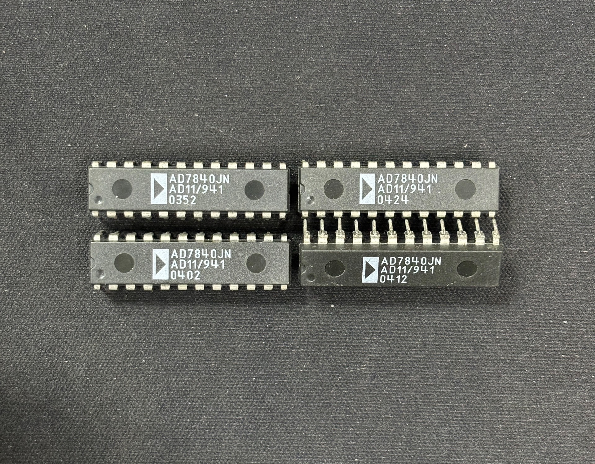
AD7840JN

Complete 14-bit voltage output DAC, ±3V bipolar, parallel/serial interface, 24-DIP, ADI AD7840JN

1800

Effective Inventory

Image for reference only

Manufacturer Part:

AD7840JN

Package:

24-Pin Plastic DIP (PDIP-24), through hole

Brand:

Product Categories:

Quality Commitment

Shipping & Payment

Service & Packaging

Product Manual

Other recommendations you may be interested in.

Description

Product Overview

The AD7840JN is a complete 14-bit voltage-output digital-to-analog converter (DAC) from Analog Devices, fabricated in LC²MOS (Linear Compatible CMOS) technology that combines precision bipolar circuits with low-power CMOS logic. Housed in a 24-pin plastic DIP package, this device integrates a 14-bit DAC, a 3V buried zener voltage reference, a DAC output amplifier, and high-speed control logic on a single chip. It features double-buffered interface logic with a 14-bit input latch and a 14-bit DAC latch, supporting both parallel and serial data loading modes. With a fast 21 ns data setup time and 45 ns minimum WR pulse width, the AD7840 interfaces directly with high-speed digital signal processors such as the ADSP-2100 and TMS320 series. The bipolar output provides ±3 V nominal range, and the device is fully specified for dynamic performance including 80 dB signal-to-noise ratio. Operating from ±5 V supplies with typical power dissipation of 70 mW, the AD7840JN is ideal for industrial control, instrumentation, and automatic test equipment applications.

Key Specifications

Parameter Value
Manufacturer Analog Devices Inc. (ADI)
Part Number AD7840JN (AD7840JNZ)
Product Type 14-Bit Voltage Output DAC
Resolution 14 bits
Number of DAC Channels 1
Architecture R-2R ladder, voltage mode
Output Type Voltage output, buffered
Output Range ±3 V (bipolar, nominal)
Settling Time 4 μs (typical, to 0.003%)
INL (Max) ±2 LSB
DNL (Max) ±1 LSB, monotonic
Signal-to-Noise Ratio 80 dB typ, 76 dB min
Full-Scale Error ±10 LSB
Reference On-chip 3 V buried zener (±5%)
Data Interface Parallel (14-bit) and Serial (up to 6 MHz)
Double Buffering Yes (input latch + DAC latch)
Supply Voltage ±4.75 V to ±5.25 V (dual ±5 V supplies)
Power Dissipation 70 mW typical, 100 mW max
Output Short-Circuit Current 20 mA typical
Glitch Impulse 10 nV·s typical
Operating Temperature 0°C ~ +70°C (commercial grade)
Package / Case 24-Pin Plastic DIP (PDIP, through-hole)
Mounting Type Through Hole
RoHS RoHS Compliant
Product Status Active

Features

  • Complete 14-bit voltage-output DAC on a single chip
  • Integrated 3V buried zener reference
  • On-chip output buffer amplifier
  • Parallel and serial interface capability
  • Double-buffered data latches (input + DAC)
  • Fast 45ns min WR pulse width
  • Direct interface to DSPs (ADSP-2100, TMS320)
  • Serial clock rate up to 6 MHz
  • 80 dB signal-to-noise ratio (typ)
  • Bipolar output: ±3 V full scale
  • Monotonic over full temperature range
  • Low power: 70 mW typical
  • LC²MOS (Linear Compatible CMOS) technology
  • Four serial data format options
  • 24-pin plastic DIP package
  • RoHS compliant version available

Applications

  • Digital signal processing (DSP) systems
  • Industrial process control and automation
  • Automatic test equipment (ATE)
  • Programmable voltage sources
  • Precision instrumentation
  • Data acquisition systems
  • Servo motor control
  • Waveform generation
  • Analog calibration circuits
  • General-purpose 14-bit DAC applications
Product Introduction: AD7840JN Product Introduction

The AD7840JN is a complete 14-bit voltage-output digital-to-analog converter manufactured by Analog Devices using proprietary LC²MOS (Linear Compatible CMOS) technology — an advanced mixed-signal process that integrates precision bipolar analog circuitry with low-power CMOS digital logic on a single die. The AD7840 provides a fully self-contained DAC solution: it includes a 14-bit R-2R ladder DAC, a 3V buried zener reference voltage source, a precision output buffer amplifier, and a complete digital control interface with double-buffered latch architecture. The double-buffered structure — consisting of a 14-bit input latch and a 14-bit DAC latch — allows new data to be loaded into the input register while the DAC maintains its current output, then simultaneously updates the DAC output under control of the LDAC (Load DAC) pin. This is essential for systems where multiple DACs must update simultaneously. The device supports both parallel and serial data loading: in parallel mode, 14 bits of data are written directly via the data bus with fast 21ns setup time, enabling direct connection to 16-bit microprocessors and DSPs; in serial mode, data is clocked in at rates up to 6 MHz with four different data format options (MSB-first/LSB-first, left-justified/right-justified). The analog output provides a true bipolar range of ±3V from a 3V reference, generated using internal bipolar offset circuitry. The AD7840 is fully characterized for dynamic performance parameters including signal-to-noise ratio (80dB typ) and total harmonic distortion, making it suitable for audio and waveform generation applications as well as traditional DC control functions. With only 70mW typical power consumption from ±5V supplies and a compact 24-pin DIP footprint, the AD7840JN remains a versatile choice for industrial control, ATE, and instrumentation applications that require a complete, standalone 14-bit DAC solution.

Working Principle: AD7840JN Working Principle

The AD7840 is a 14-bit voltage-mode DAC based on an R-2R (resistor ladder) architecture. The DAC section consists of a network of precision thin-film resistors in an R-2R ladder configuration, with NMOS single-pole double-throw switches that connect each ladder rung to either the reference voltage or ground depending on the corresponding bit value. The three MSBs use a segmented architecture with seven separate switch groups driven by a 3-bit decoder, while the remaining 11 LSBs use a conventional R-2R ladder structure. The output of the resistor network is a current that is proportional to the digital input code and the reference voltage; this current is converted to a voltage by the internal output amplifier. The on-chip 3V buried zener reference provides a stable, low-drift voltage reference for the DAC — buried zener references achieve excellent long-term stability and low temperature coefficient compared to bandgap references. The bipolar output range of ±3V is achieved by offsetting the unipolar DAC output with a precision reference-derived bias voltage, so that a mid-scale digital input (code 2000H for 14 bits) produces 0V output, full-scale produces +3V, and zero-scale produces -3V. The double-buffered latch structure consists of two cascaded registers: the input latch receives new data from the parallel or serial interface when WR is asserted, and the DAC latch transfers the input latch data to the DAC when LDAC is asserted. This two-stage architecture allows pre-loading of new data while the current output is maintained, and enables synchronous updates across multiple DACs when their LDAC pins are tied together. The overall device operates from dual ±5V supplies, with the analog and digital sections separated to minimize noise coupling.

Pin Description: AD7840JN Pin Definition and Functions

The AD7840JN is packaged in a 24-pin plastic DIP (PDIP-24). Key pin assignments:

Pin Name Type Description
1 VDD Power Positive power supply (+5V ±5%)
2-6 DB13-DB9 Input Parallel data bits 13 through 9 (MSB side)
7 FORMAT Input Serial format select (MSB-/LSB-first)
8 JUSTIFY Input Serial data justification select
9 SCLK Input Serial clock input (up to 6 MHz)
10 SDIN Input Serial data input
11 LDAC Input Load DAC (asynchronous, active low)
12 WR Input Write input (active low, 45ns min pulse)
13 CS Input Chip select (active low)
14 REF IN Input Reference input (2.85V to 3.15V)
15 VSS Power Negative power supply (-5V ±5%)
16 AGND Ground Analog ground
17 VOUT Output DAC analog voltage output (±3V range)
18 DGND Ground Digital ground
19-23 DB0-DB4 Input Parallel data bits 0 through 4 (LSB side)
24 DB5/DB8* Input Parallel data bit 5 / BYTE SEL (mode dependent)

Note: DB5 through DB13 serve as the 14-bit parallel data bus; some pins serve dual functions depending on PAR/SER mode. Please consult the full datasheet for complete pin descriptions and timing specifications.

Application Scenarios: In which products and applications is AD7840JN used
  • Digital Signal Processing (DSP) Systems: Used as the analog output front-end in DSP-based systems for audio processing, filtering, and waveform generation, leveraging the fast parallel interface that directly connects to ADSP-2100 and TMS320 series DSPs
  • Industrial Process Control: Provides precise analog control voltages for PID controllers, valve positioners, temperature controllers, and other industrial automation equipment requiring 14-bit resolution setpoint generation
  • Automatic Test Equipment (ATE): Used in semiconductor test systems, board-level testers, and calibration equipment to generate programmable reference voltages and bias signals with high accuracy
  • Programmable Voltage Sources: Forms the core of digitally controlled power supplies, voltage calibrators, and laboratory bench instruments where precise, software-programmable analog outputs are required
  • Servo and Motor Control: Generates analog command signals for servo amplifiers, motor drives, and positioning systems, providing smooth 14-bit resolution control with low glitch
  • Waveform and Function Generation: Used in arbitrary waveform generators and function generators where the 80dB SNR and 20kHz full-power bandwidth support high-quality analog waveform synthesis
  • Precision Instrumentation: Found in oscilloscopes, multimeters, and data loggers for offset adjustment, gain control, and trigger level generation
  • Data Acquisition Output Stages: Serves as the analog output channel in bidirectional data acquisition systems, providing the DAC counterpart to ADC inputs in closed-loop control and monitoring systems
Alternative Models: What chips are recommended as replacements for AD7840JN
Part Number Manufacturer Resolution Output Interface Package
AD7840JN ADI 14-bit ±3V voltage Parallel/Serial 24-DIP
AD7840JPZ ADI 14-bit ±3V voltage Parallel/Serial 28-PLCC
AD7840ARSZ ADI 14-bit ±3V voltage Parallel/Serial 24-SSOP
AD558 ADI 8-bit 0-10V voltage Parallel 16-DIP
DAC8043 TI/Burr-Brown 12-bit Voltage output SPI 8-SOIC
DAC8811 TI 16-bit Voltage output SPI SOT-23

Recommend Parts

RK73B2ATTD100J

10Ohm +/-5% 0.125W thick film resistor, 0805, +/-200 ppm/C, AEC-Q200

Brand: KOA Speer

Package: 0805 (2012 Metric) 2.0 x 1.25 x 0.55 mm

IN STOCK: 26435pcs

Cargo cycle: 3-7 Days

The minimum order is 1

TPS77001DBVR

50mA LDO, adjustable 1.2-5.5V out, 35mV dropout, 17µA IQ, SOT-23-5

Brand: TI

Package: SOT-23-5 (2.9 x 1.6 x 1.45 mm)

IN STOCK: 5000pcs

Cargo cycle: 3-7 Days

The minimum order is 1

TPL5010DDCR

Nano-power watchdog timer with power good, SOT-23-6

Brand: TI

Package: SOT-23-6 (2.9 x 1.6 x 1.1 mm, DDC package)

IN STOCK: 12122pcs

Cargo cycle: 3-7 Days

The minimum order is 1

S1MB-13-F

1A 1000V GPP rectifier, 1.1V VF, 3μs trr, SMB/DO-214AA, -65~150°C

Brand: Diodes Inc

Package: SMB / DO-214AA (4.57 x 3.94 x 2.50mm)

IN STOCK: 3679pcs

Cargo cycle: 3-7 Days

The minimum order is 1

WS2811

3-channel LED driver IC with built-in oscillator, SOP-8

Brand: Worldsemi

Package: SOP-8 (5.2 x 4.0 mm)

IN STOCK: 7374pcs

Cargo cycle: 3-7 Days

The minimum order is 1

AD9912ABCPZ

1GSPS direct digital synthesizer with 14-bit DAC, LFCSP-64

Brand: ADI

Package: LFCSP-64 (9.0 x 9.0 mm, BCPZ package)

IN STOCK: 3719pcs

Cargo cycle: 3-7 Days

The minimum order is 1