

Opens in a new tab

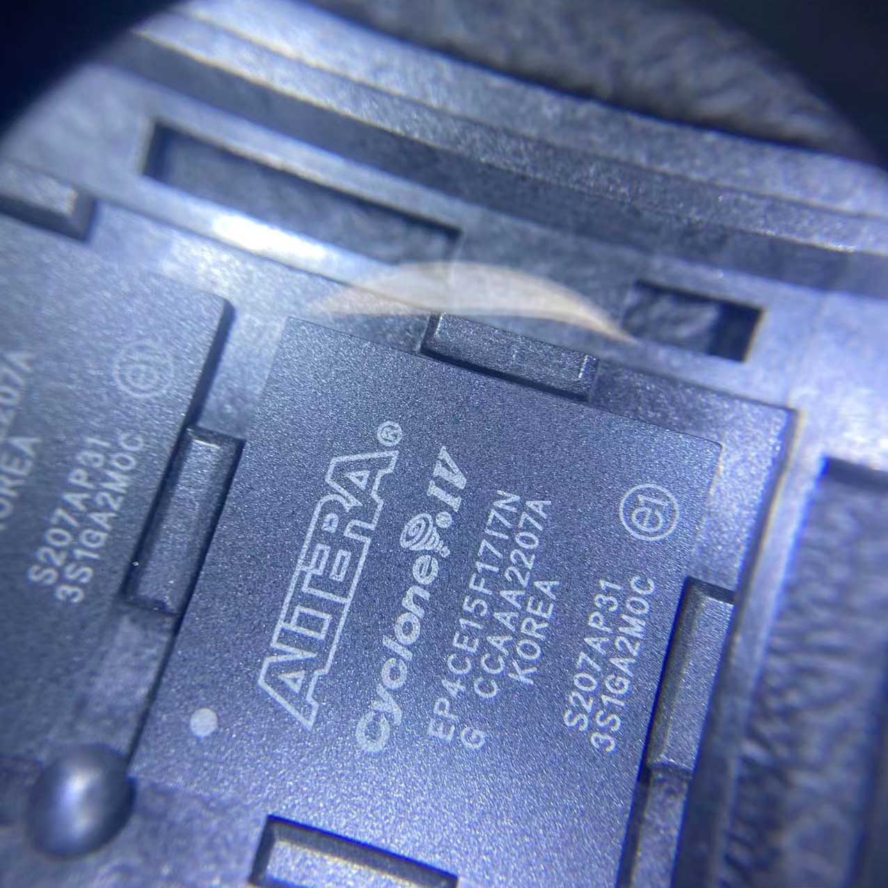
EP4CE15F17I7N

Cyclone IV E FPGA, 15408 LE, 516Kb RAM, 56 multipliers, 4 PLLs, industrial -40~100°C, 256-FBGA, Altera EP4CE15F17I7N

1650

Effective Inventory

Image for reference only

Manufacturer Part:

EP4CE15F17I7N

Package:

256-Pin FineLine BGA (FBGA256, 17mm × 17mm), surface mount

Brand:

Product Categories:

Quality Commitment

Shipping & Payment

Service & Packaging

Product Manual

Other recommendations you may be interested in.

Description

Product Overview

The EP4CE15F17I7N is a field-programmable gate array from Altera (now Intel) Cyclone® IV E family, offering a cost-optimized combination of logic, memory, and DSP resources with low power consumption. Housed in a 256-pin FineLine BGA package (17×17mm), this industrial-grade device features 15,408 logic elements (LEs), 56 M9K RAM blocks totaling 516 Kbits of embedded memory, 56 embedded 18×18 multipliers, 4 phase-locked loops (PLLs), 20 global clock networks, and up to 181 user I/O pins. Built on TSMC’s 60nm low-power process technology with a 1.0V/1.2V core, Cyclone IV E devices deliver the lowest static power in the Cyclone family. The -7 speed grade and industrial temperature range (-40°C to +100°C) make this device suitable for industrial control, automotive, communications, and consumer applications requiring reliable operation at low cost and low power.

Key Specifications

Parameter Value
Manufacturer Altera (Intel® PSG)
Part Number EP4CE15F17I7N
Product Family Cyclone® IV E
Product Type Field Programmable Gate Array (FPGA)
Logic Elements (LEs) 15,408
Logic Array Blocks (LABs) 963 (16 LEs per LAB)
Embedded Memory (M9K Blocks) 56 blocks (9,216 bits each)
Total RAM Bits 516 Kbits (516,096 bits)
Embedded Multipliers 56 (18 × 18-bit multipliers)
Phase-Locked Loops (PLLs) 4
Global Clock Networks 20
Maximum User I/O Pins Up to 181 (256-pin FBGA, 17×17)
Core Voltage 1.0 V / 1.2 V (variable / fixed)
I/O Voltage Support 3.3 V, 2.5 V, 1.8 V, 1.5 V, 1.2 V
I/O Standards LVTTL, LVCMOS, SSTL, HSTL, PCI, LVDS, etc.
Differential Channels Up to 72 LVDS channels
External Memory Support DDR/DDR2 SDRAM, SDR SDRAM
DDR2 Interface Speed Up to 167 MHz (333 Mbps)
Configuration Modes AS, AP, PS, FPP, JTAG
Speed Grade -7 (I7 = Industrial grade, speed 7)
Operating Temperature -40°C ~ +100°C (industrial, I grade)
Package / Case 256-Pin FineLine BGA (FBGA256, 17mm × 17mm)
Mounting Type Surface Mount
Process Technology 60 nm TSMC low-power
RoHS RoHS Compliant
MSL Level MSL 3 (168 hours)
Product Status Active

Features

  • Lowest cost, low-power Cyclone IV E FPGA family
  • 15,408 logic elements (LEs) for custom logic
  • 516 Kbits of embedded SRAM (56 × M9K blocks)
  • 56 embedded 18×18 multipliers for DSP applications
  • 4 phase-locked loops (PLLs) for clock management
  • 20 global clock networks
  • Up to 181 user I/O pins (256-FBGA)
  • Single-ended I/O: LVTTL, LVCMOS 3.3/2.5/1.8/1.5/1.2V
  • Differential I/O: LVDS, mini-LVDS, RSDS, LVPECL
  • External memory: DDR2, DDR, SDR SDRAM
  • DDR2 up to 333 Mbps (167 MHz)
  • Nios II soft embedded processor support
  • Comprehensive IP core library
  • 1.0V / 1.2V core voltage for lowest power
  • Multiple I/O banks with independent voltage
  • 60 nm TSMC low-power process technology
  • Configuration: serial flash, parallel flash, JTAG
  • Industrial temperature range: -40°C ~ +100°C
  • 256-pin FineLine BGA (17mm × 17mm)
  • RoHS compliant, MSL 3
  • High value for high-volume designs

Applications

  • Industrial control and automation
  • Automotive electronics
  • Video processing and display systems
  • Communications equipment
  • Consumer electronics
  • Motor control and drives
  • Nios II soft processor systems
  • Image and signal processing
  • Test and measurement equipment
  • Cost-sensitive, low-power FPGA designs
Product Introduction: EP4CE15F17I7N Product Introduction

The EP4CE15F17I7N is an industrial-grade FPGA from Altera’s Cyclone IV E family — the fourth generation of Cyclone low-cost FPGAs, specifically engineered to deliver the lowest possible cost and power consumption for high-volume applications. Manufactured on TSMC’s 60nm low-power process technology with core options of 1.0V (for lowest power) or 1.2V (for highest performance), Cyclone IV E devices set a benchmark for low static power consumption while still providing substantial logic, memory, and DSP resources. The EP4CE15 variant provides 15,408 logic elements — a medium-sized configuration that balances resource availability with cost efficiency for a wide range of applications. The ‘F17’ indicates a 256-pin FineLine BGA package with 17mm body size, and ‘I7N’ denotes industrial temperature range (-40°C to +100°C junction temperature) with -7 speed grade. The logic architecture is built on refined logic elements containing 4-input look-up tables and programmable registers, organized into 963 logic array blocks (LABs) of 16 LEs each. The memory subsystem includes 56 M9K RAM blocks, each 9,216 bits, totaling 516 Kbits of on-chip memory configurable as single-port, dual-port, FIFO, shift register, or ROM. For digital signal processing, 56 embedded 18×18-bit multipliers provide dedicated hardware multiplication resources for efficient implementation of FIR filters, FFTs, and other DSP functions. Four phase-locked loops (PLLs) offer flexible clock synthesis with frequency multiplication/division, phase shifting, and spread-spectrum clocking capabilities. Twenty global clock networks provide robust, low-skew clock distribution across the device. The 256-pin FBGA package offers up to 181 user I/O pins organized into multiple independent I/O banks, supporting a comprehensive set of single-ended and differential I/O standards including LVDS at up to 805 Mbps. External memory interfaces support DDR2 SDRAM at up to 167 MHz (333 Mbps), as well as DDR and SDR SDRAM. The Cyclone IV E family is fully supported by Altera’s Quartus II design software and the extensive library of Altera IP cores including the Nios II soft embedded processor, DDR memory controllers, Ethernet MACs, and numerous DSP and interface functions. With its combination of low cost, low power, industrial temperature rating, and balanced resources, the EP4CE15F17I7N is ideal for cost-sensitive industrial, automotive, consumer, and communications applications.

Working Principle: EP4CE15F17I7N Working Principle

The Cyclone IV E FPGA is an SRAM-based programmable logic device whose internal configuration is determined by data stored in static memory cells throughout the device. At power-up, the FPGA has no defined functionality — it must be configured by loading a bitstream that programs the logic elements, routing resources, I/O buffers, and memory blocks. Configuration can occur through several modes: Active Serial (AS) mode where the FPGA reads configuration data from an external serial flash device (EPCS or EPCQ series); Active Parallel (AP) mode for parallel Flash memory; Passive Serial (PS) or Fast Passive Parallel (FPP) mode where an external controller provides configuration data; or via the JTAG interface for in-system programming and debugging. The logic core is built from logic elements (LEs), each containing a 4-input look-up table (LUT) that can implement any Boolean function of up to 4 variables, plus a programmable flip-flop that can be configured as D, T, JK, or SR flip-flop for sequential logic. Carry chains enable efficient implementation of arithmetic functions like adders and counters. LEs are grouped into sets of 16 called logic array blocks (LABs), with each LAB having dedicated local interconnect for fast intra-LAB communication. The M9K memory blocks are 9,216-bit true dual-port SRAM blocks with various configuration options: single-port RAM, simple dual-port RAM, true dual-port RAM, shift register (RAM-based), ROM (with initialization data), or FIFO buffer (with almost-full/empty flags). Each embedded multiplier block contains an 18×18-bit multiplier that supports both signed and unsigned operations. These blocks can also be divided into two independent 9×9 multipliers for lower-precision applications, effectively doubling the multiplier count for DSP designs that don’t need full 18-bit precision. The four PLLs provide advanced clock synthesis including frequency multiplication and division, phase shifting with fine resolution, spread-spectrum clocking for electromagnetic interference (EMI) reduction, and clock switchover for clock redundancy applications. Twenty global clock networks with clock control blocks at the center of the device distribute clock signals with minimal skew to all regions of the FPGA. The I/O elements (IOEs) at the periphery provide configurable input/output buffers with support for many I/O standards, programmable drive strength, slew rate control, bus-hold, and pull-up/down resistors. Differential I/O buffers support LVDS and other differential standards for high-speed serial data transfer. The overall architecture provides a flexible fabric that can implement virtually any digital logic function — from simple state machines to complete systems-on-chip with Nios II processors, memory interfaces, and custom hardware accelerators.

Pin Description: EP4CE15F17I7N Pin Definition and Functions

The EP4CE15F17I7N is available in a 256-pin FineLine BGA package (17mm × 17mm body size). Major pin groups:

Pin Group Approx. Count Description
Core Power Pins ~30 VCCINT (1.0V or 1.2V core supply)
I/O Power Pins ~16 VCCIO (I/O bank supplies, 2.5V/3.3V/1.8V/1.5V/1.2V)
PLL Power Pins ~8 VCCA_PLL (PLL analog supply), VCCD_PLL (PLL digital)
Ground Pins ~50 GND (multiple for power distribution and signal integrity)
User I/O Pins Up to 181 General-purpose I/O, organized into 8 I/O banks
I/O Bank 1 ~24 Top-left I/O bank
I/O Bank 2 ~24 Bottom-left I/O bank
I/O Bank 3 ~24 Top-right I/O bank
I/O Bank 4 ~24 Bottom-right I/O bank
I/O Bank 5 ~21 Top I/O bank
I/O Bank 6 ~21 Bottom I/O bank
I/O Bank 7 ~22 Left-side middle bank
I/O Bank 8 ~21 Right-side middle bank
Clock Inputs 16 CLK[0..15] dedicated clock pins
PLL Outputs 8 PLL external clock outputs (PLL1~4_OUTp/m)
LVDS Pairs ~36 diff pairs Differential I/O pairs (left and right banks)
Configuration Pins ~12 nCONFIG, nSTATUS, CONF_DONE, DCLK, DATA0, nCE, nCSO, ASDO, etc.
JTAG Pins 4 TCK, TMS, TDI, TDO (JTAG test/configuration)
Test Pins 2 TEST_IN, TEST_OUT (factory test)

Note: Exact I/O count depends on power/ground pin count and dedicated function pins. Refer to the official Cyclone IV E EP4CE15 datasheet, Quartus II pin planner, and device pin files for complete pin assignments, I/O bank voltage assignments, and electrical specifications.

Application Scenarios: In which products and applications is EP4CE15F17I7N used
  • Industrial Control & Automation: Used in PLC I/O modules, industrial sensor signal processing, motion controllers, and factory automation systems where the industrial temperature rating ensures reliable operation in harsh factory environments with varying temperatures
  • Automotive Electronics: Deployed in automotive infotainment systems, body electronics modules, and driver assistance camera processing (with AEC-Q100 variants), leveraging the -40°C to +100°C range for automotive operating conditions
  • Video Processing & Displays: Used in flat-panel display controllers, video scalers, format converters, and video processing pipelines where parallel pixel processing, display timing generation, and low cost are key requirements
  • Communications Equipment: Found in network access equipment, protocol converters, wireless base stations, and optical transport modules for packet processing, PHY interfaces, and protocol bridging functions
  • Consumer Electronics: Used in set-top boxes, gaming accessories, digital TV peripherals, and smart home devices where low cost, low power, and high-volume manufacturability are critical success factors
  • Motor Control & Drives: Used in industrial motor drives, servo controllers, and power converters for high-speed PWM generation, current loop processing, encoder interfaces, and custom control logic acceleration
  • Nios II Soft Processor Systems: Implements complete Nios II embedded processor systems with custom peripherals, memory interfaces, and hardware accelerators — providing a flexible software-programmable platform at FPGA cost points
  • Test & Measurement: Deployed in data acquisition systems, oscilloscopes, logic analyzers, and custom test equipment for high-speed data capture, real-time signal processing, and custom trigger logic implementation
Alternative Models: What chips are recommended as replacements for EP4CE15F17I7N
Part Number Manufacturer LEs RAM (Kb) Multipliers Temp/Grade
EP4CE15F17I7N Altera/Intel 15,408 516 56 -40~100°C / Industrial
EP4CE15F17C6N Altera/Intel 15,408 516 56 0~85°C / Commercial
EP4CE10F17I7N Altera/Intel 10,320 423 46 -40~100°C / Industrial
EP4CE22F17I7N Altera/Intel 22,320 608 66 -40~100°C / Industrial
EP3C16F256I7N Altera/Intel 15,408 516 56 -40~100°C / Cyclone III
XC6SLX16-3FTG256I Xilinx 14,579 227 32 -40~100°C / Industrial

Recommend Parts

RK73B2ATTD100J

10Ohm +/-5% 0.125W thick film resistor, 0805, +/-200 ppm/C, AEC-Q200

Brand: KOA Speer

Package: 0805 (2012 Metric) 2.0 x 1.25 x 0.55 mm

IN STOCK: 26435pcs

Cargo cycle: 3-7 Days

The minimum order is 1

TPS77001DBVR

50mA LDO, adjustable 1.2-5.5V out, 35mV dropout, 17µA IQ, SOT-23-5

Brand: TI

Package: SOT-23-5 (2.9 x 1.6 x 1.45 mm)

IN STOCK: 5000pcs

Cargo cycle: 3-7 Days

The minimum order is 1

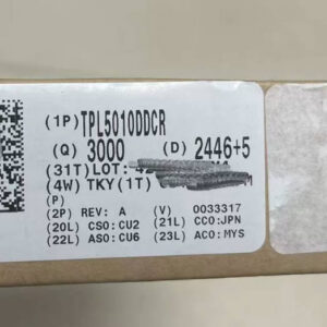
TPL5010DDCR

Nano-power watchdog timer with power good, SOT-23-6

Brand: TI

Package: SOT-23-6 (2.9 x 1.6 x 1.1 mm, DDC package)

IN STOCK: 12122pcs

Cargo cycle: 3-7 Days

The minimum order is 1

S1MB-13-F

1A 1000V GPP rectifier, 1.1V VF, 3μs trr, SMB/DO-214AA, -65~150°C

Brand: Diodes Inc

Package: SMB / DO-214AA (4.57 x 3.94 x 2.50mm)

IN STOCK: 3679pcs

Cargo cycle: 3-7 Days

The minimum order is 1

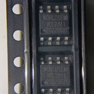
WS2811

3-channel LED driver IC with built-in oscillator, SOP-8

Brand: Worldsemi

Package: SOP-8 (5.2 x 4.0 mm)

IN STOCK: 7374pcs

Cargo cycle: 3-7 Days

The minimum order is 1

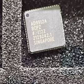
AD9912ABCPZ

1GSPS direct digital synthesizer with 14-bit DAC, LFCSP-64

Brand: ADI

Package: LFCSP-64 (9.0 x 9.0 mm, BCPZ package)

IN STOCK: 3719pcs

Cargo cycle: 3-7 Days

The minimum order is 1