
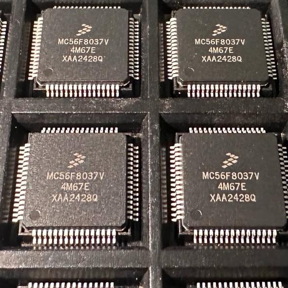
The MC56F8037VLH from NXP Semiconductors (formerly Freescale) is a 16-bit 56800E core Digital Signal Controller (DSC) in a 64-pin LQFP package. It features 32 MHz core frequency (32 MIPS), 64 KB program Flash, 8 KB unified data/program RAM, dual Harvard architecture, 6-channel PWM with 96 MHz operating clock, two 12-bit ADCs (2.67 MSPS), two 12-bit DACs, two QSCI, two QSPI, one I2C, one MSCAN, two Quad Timers, three PITs, and two analog comparators. Operating voltage is 3.0-3.6 V with temperature range -40C to +105C.
Home » Clock & Timing ICs, Integrated Circuits ICs » MC56F8037VLH
MC56F8037VLH
16-bit 56800E DSC, 32MHz, 64KB Flash, 8KB RAM, 6-ch PWM, 2xADC, 2xDAC, CAN, LQFP64
956
Effective Inventory
Manufacturer Part:
MC56F8037VLH
Package:
64-LQFP (10 x 10 x 1.4 mm, 0.5mm pitch, gull-wing)
Brand:
Product Categories:
Quality Commitment
Shipping & Payment
Service & Packaging
Product Manual
Other recommendations you may be interested in.
Description
Product Introduction: MC56F8037VLH Product Introduction
The MC56F8037VLH from NXP Semiconductors (formerly Freescale) is a 16-bit Digital Signal Controller (DSC) that combines digital signal processing and microcontroller functionalities on a single chip. It is based on the 56800E core, a dual Harvard-style architecture with three parallel execution units that can perform up to six operations per instruction cycle.
The 56800E core operates at 32 MHz, delivering 32 MIPS performance. It features a single-cycle 16×16-bit parallel MAC (Multiply-Accumulate), four 36-bit accumulators with extension bits, a 32-bit ALU with multi-bit shifter, hardware DO and REP loops, and parallel instruction set with unique DSP addressing modes. The MCU-style programming model and optimized instruction set support efficient C compiler output for rapid development.
Memory includes 64 KB (32K x 16) program Flash with page erase (512 bytes/page) and security/protection features, plus 8 KB (4K x 16) unified data/program RAM. The dual Harvard architecture allows up to three simultaneous memory accesses per instruction cycle. EEPROM emulation is possible using the Flash.
The 6-channel PWM module operates at up to 96 MHz clock with 15-bit resolution, supporting both center-aligned and edge-aligned modes. Four programmable fault inputs with digital filters provide protection. The PWM outputs can be sourced from the PWM generator, external GPIO, internal timers, analog comparators, or ADC limit comparisons.
Two independent 12-bit ADCs provide 2 x 8 channels with simultaneous and sequential conversion support, synchronized by PWM and timer modules at up to 2.67 MSPS. Two 12-bit DACs feature 2 us settling time and automatic waveform generation (square, triangle, sawtooth).
Communication peripherals include two QSCI (UART with LIN slave), two QSPI, one I2C (400 kbps), and one MSCAN (CAN 2.0A/B, up to 1 Mbps, 5 RX + 3 TX buffers). Two Quad Timer modules provide eight 16-bit counter/timers with 12 operating modes each.
The MC56F8037VLH includes 53 GPIO pins with 5 V tolerance, JTAG/OnCE debug interface, on-chip regulators, PLL, internal relaxation oscillator, and power management (Wait and Stop modes). The 64-LQFP package measures 10 x 10 mm.
Note: NXP designates the 56F803X family as “Not Recommended for New Designs” (NRND). The product is included in NXP’s product longevity program with assured supply for a minimum of 10 years after launch. Designers should consider the MC56F837xx or Kinetis KV series for new designs.
Working Principle: MC56F8037VLH Working Principle
**56800E DSC Core:** The 56800E core uses a modified dual Harvard architecture with separate program and data memory buses, allowing up to three simultaneous memory accesses per instruction cycle. Three execution units operate in parallel: Data ALU, Address Generation Unit (AGU), and Program Controller. This enables up to six operations per instruction (1 data ALU, 2 address calculations, 2 data moves, 1 program control).
**MAC and Accumulators:** The 16×16-bit MAC performs single-cycle multiply-accumulate operations. Four 36-bit accumulators (with 4-bit extension) provide headroom for iterative calculations without overflow. The parallel instruction set supports MAC with parallel data moves, enabling efficient FIR/IIR filter implementation.
**Dual Harvard Memory:** Program memory (Flash) and data memory (RAM) are accessed through separate buses. The program bus fetches instructions (and optional data via program space), while the data bus reads/writes operands. This dual-bus architecture eliminates the Von Neumann bottleneck.
**PWM Module:** The 6-channel PWM module generates complementary PWM signals with programmable dead time, supporting 3-phase motor drive. The 96 MHz PWM clock provides 15-bit resolution at typical motor drive frequencies (e.g., 20 kHz PWM = 15-bit duty cycle resolution). The four fault inputs can immediately disable PWM outputs for overcurrent protection.
**ADC Synchronization:** The ADC modules can be synchronized to PWM reload events via the Quad Timer module, ensuring that current sensing occurs at the optimal point in the PWM cycle (typically at PWM center for minimum ripple). This hardware synchronization eliminates the need for software-timed ADC triggers.
Pin Description: MC56F8037VLH Pin Definition and Functions
| Pin Group | Name | Type | Description |
|---|---|---|---|
| Multiple | VDD | P | Digital supply; 3.0-3.6V; powers core and digital logic; decouple with 100nF + 10uF; on-chip regulator generates internal 2.5V and 1.8V |
| Multiple | VSS | G | Digital ground; connect to ground plane; reference for digital I/O |
| Dedicated | VDDA | P | Analog supply; 3.0-3.6V; powers ADC, DAC, comparators, PLL; must be clean and stable; separate from VDD via ferrite bead; decouple with 100nF + 1uF |
| Dedicated | VSSA | G | Analog ground; return for ADC/DAC; connect to ground plane at single point |
| 6 | PWM0-PWM5 | O | PWM outputs; 6 channels; complementary pairs with dead-time; up to 96MHz clock; 15-bit resolution; fault-protected; configurable as GPIO; 5V tolerant |
| 16 | ADC0-ADC15 | I | Analog inputs; 2×8 channels (ADCA and ADCB); 12-bit; 2.67 MSPS; simultaneous or sequential; 5V tolerant when configured as digital input |
| 2 | DACA/DACB | O | DAC outputs; 12-bit; 2us settling time; 0 to VDDA range; automatic waveform generation; can drive analog comparator inputs |
| 2 | TXD/RXD (QSCI) | I/O | QSCI serial communication; two independent UARTs with LIN slave; full-duplex; 4-byte TX and RX FIFOs; up to 3.125 Mbps |
| 4 | MOSI/MISO/SS/SCK (QSPI) | I/O | QSPI communication; two independent SPI controllers; master/slave; 4-word TX and RX FIFOs; programmable 2-16 bit transactions |
| 2 | SDA/SCL (I2C) | I/O | I2C interface; up to 400 kbps; master and slave; 10-bit addressing; broadcast mode |
| 2 | CANRX/CANTX | I/O | MSCAN interface; CAN 2.0A/B; up to 1 Mbps; 5 RX + 3 TX buffers; standard and extended frames |
| 53 | GPIO | I/O | General-purpose I/O; 5V tolerant; individually configurable as input/output; shared with peripheral functions; internal pull-ups on some pins |
| Dedicated | RESET | I | Active-low reset; Schmitt trigger; external pull-up recommended; internal POR and LVI; assert for minimum 4 core clock cycles |
| Dedicated | TCK/TMS/TDI/TDO | I/O | JTAG/OnCE debug interface; 4-pin boundary scan and real-time debug; connect to JTAG header; TDI pull-up recommended |
Application Scenarios: In which products and applications is MC56F8037VLH used
| Application | Description |
|---|---|
| 3-Phase BLDC/PMSM Motor Control | FOC or trapezoidal commutation for BLDC/PMSM motors; 6-ch PWM generates 3-phase drive with complementary signals and dead-time; 2x ADC for simultaneous phase current sensing synchronized to PWM; MAC for Park/Clarke transforms; CAN for fieldbus communication |
| Solar Inverter / SMPS | Digital control of switch-mode power supplies and solar micro-inverters; high-resolution PWM for precise duty cycle; 2x ADC for voltage/current feedback; DAC for reference generation; comparators for fast overcurrent protection |
| Home Appliance Motor Drive | Variable-speed motor control in washing machines, refrigerators, and HVAC compressors; 32 MIPS sufficient for simple FOC; CAN for appliance communication; I2C for sensor interface; low cost compared to 32-bit alternatives |
Alternative Models: What chips are recommended as replacements for MC56F8037VLH
| Model | Manufacturer | Compatibility | Key Difference |
|---|---|---|---|
| MC56F8027VLH | NXP | Lower Cost Variant | Same 56800E core and peripherals; 32KB Flash (half); 4KB RAM (half); same LQFP64 pinout; drop-in for designs that fit in smaller memory; lower cost |
| MPC56F8377VLH | NXP | Higher Performance Upgrade | 56800EX core (enhanced); 60 MHz; 256KB Flash; 32KB RAM; more PWM channels; Ethernet; same DSC architecture; use for designs needing more performance/memory |
| MKE16F256VLF | NXP | Modern Alternative (Kinetis) | ARM Cortex-M4F; 72 MHz; 256KB Flash; 32KB RAM; 2x CAN; LQFP64; Kinetis KV family; recommended for new designs; ARM ecosystem |
Recommend Parts
RK73B2ATTD100J
10Ohm +/-5% 0.125W thick film resistor, 0805, +/-200 ppm/C, AEC-Q200
Brand: KOA Speer
Package: 0805 (2012 Metric) 2.0 x 1.25 x 0.55 mm
IN STOCK: 26435pcs
Cargo cycle: 3-7 Days
The minimum order is 1

TPS77001DBVR
50mA LDO, adjustable 1.2-5.5V out, 35mV dropout, 17µA IQ, SOT-23-5
Brand: TI
Package: SOT-23-5 (2.9 x 1.6 x 1.45 mm)
IN STOCK: 5000pcs
Cargo cycle: 3-7 Days
The minimum order is 1
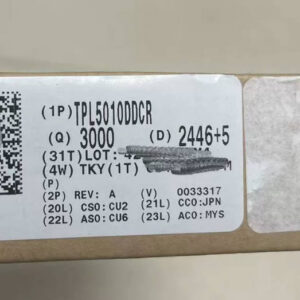
TPL5010DDCR
Nano-power watchdog timer with power good, SOT-23-6
Brand: TI
Package: SOT-23-6 (2.9 x 1.6 x 1.1 mm, DDC package)
IN STOCK: 12122pcs
Cargo cycle: 3-7 Days
The minimum order is 1
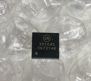
NCP302045MNTWG
45V 5A programmable overcurrent protection switch, 50mΩ Ron, -60V reverse polarity, DFN-8
Brand: ON
Package: DFN-8 (3x3mm, 0.65mm pitch)
IN STOCK: 4759pcs
Cargo cycle: 3-7 Days
The minimum order is 1
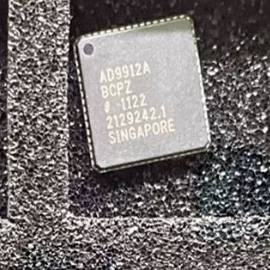
AD9912ABCPZ
1GSPS direct digital synthesizer with 14-bit DAC, LFCSP-64
Brand: ADI
Package: LFCSP-64 (9.0 x 9.0 mm, BCPZ package)
IN STOCK: 3719pcs
Cargo cycle: 3-7 Days
The minimum order is 1