Opens in a new tab

Home » Integrated Circuits ICs » 74HC4094D

74HC4094D

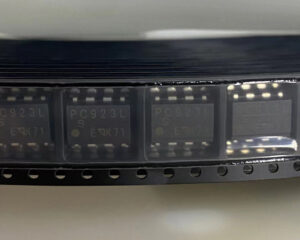
8-bit shift-and-store register, 3-state outputs, cascade capable, SOIC-16

6911

Effective Inventory

Image for reference only

Manufacturer Part:

74HC4094D

Package:

SOIC-16 (9.9 x 3.9 x 1.5 mm)

Brand:

Product Categories:

Quality Commitment

Shipping & Payment

Service & Packaging

Product Manual

Description

Product Overview

The 74HC4094D from NXP is an 8-stage serial-in/serial or parallel-out shift-and-store bus register with 3-state outputs. It operates from 2V to 6V with separate shift and storage register clocks in a 16-pin SOIC package.

Key Specifications

Function 8-Stage Shift-and-Store Bus Register
Bits 8
Supply Voltage 2V to 6V (HC)
Output Type 3-State
Propagation Delay 19ns at 5V (typ)
Max Clock Frequency 86MHz at 5V
Output Drive +/-4mA at 5V
Operating Temperature -40 to 125 C

Features

  • 8-bit serial-in, serial or parallel-out shift register
  • Separate shift register and storage register clocks
  • Two serial outputs (QS1, QS2) for cascading
  • 3-state parallel outputs for bus sharing
  • Strobe input transfers shift data to storage register
  • Output enable control (OE) for 3-state operation
  • Input clamp diodes for overvoltage protection

Applications

  • Serial-to-parallel data conversion
  • LED display driving with cascaded registers
  • Remote control holding registers
  • GPIO expansion via serial interface
  • Display multiplexing
Product Introduction: 74HC4094D Product Introduction

The 74HC4094D from NXP (formerly Nexperia) is an 8-stage serial-in/serial or parallel-out shift register with a storage register and 3-state outputs. It features separate clocks for the shift and storage registers, providing flexible data management. The device has a serial data input (D) and two serial outputs (QS1 and QS2) that enable daisy-chain cascading of multiple devices. QS1 outputs data on the rising clock edge for fast cascading, while QS2 outputs on the falling edge for slow-edge compatibility. Data is shifted through the register on LOW-to-HIGH transitions of the clock (CP) input, and transferred to the storage register when the strobe (STR) input is HIGH. The 3-state parallel outputs are controlled by the output enable (OE) pin, allowing connection to shared bus lines. Operating from 2V to 6V with CMOS input levels, the 74HC4094D is specified for -40 to 125 C in a 16-pin SOIC package.

Working Principle: 74HC4094D Working Principle

The 74HC4094D operates as a serial-to-parallel converter with intermediate storage. Key subsystems include: (1) 8-Stage Shift Register – on each rising edge of CP, data at the D input is shifted into the first stage, and existing data shifts one position toward the last stage; (2) Storage Register – when STR is HIGH, the contents of the shift register are transferred to the storage register; this allows the shift register to be loaded while the storage register holds the previous data on the outputs; (3) 3-State Output Buffers – when OE is HIGH, the storage register data appears on QP0-QP7; when OE is LOW, all outputs are in high-impedance state; (4) Cascading Outputs – QS1 provides data from the last shift register stage on the rising CP edge for fast-edge cascading; QS2 provides the same data on the falling CP edge for slow-edge cascading; (5) Input Clamp Diodes – protect inputs from voltage excursions beyond the supply rails.

Pin Description: 74HC4094D Pin Definition and Functions
Pin Name Type Function
1 STR Input Strobe (transfer shift to storage)
2 D Input Serial data input
3 CP Input Clock input (rising edge shifts)
4-7 QP0-QP3 Output Parallel outputs 0-3 (3-state)
8 VSS Power Ground
9-10 QS1/QS2 Output Serial cascade outputs
11-14 QP7-QP4 Output Parallel outputs 7-4 (3-state)
15 OE Input Output enable (active high)
16 VDD Power Supply voltage (2V to 6V)
Application Scenarios: In which products and applications is 74HC4094D used
  • Serial-to-parallel conversion: expanding MCU GPIO via 3-wire serial interface
  • LED display driving: cascading multiple 74HC4094D for large LED matrices
  • Remote control holding registers: maintaining output states in remote control applications
  • Display multiplexing: driving 7-segment or LED bar displays with minimal MCU pins
  • Industrial control: output expansion for PLC and relay driver applications
Alternative Models: What chips are recommended as replacements for 74HC4094D
Manufacturer Part Number Package Notes
TI CD74HC4094EE4 SOIC-16 Pin-compatible, TI version
Nexperia 74HCT4094D SOIC-16 TTL input levels version
TI SN74HC595DWR SOIC-16 Similar 8-bit shift register
onsemi MC74HC4094ADWR2G SOIC-16 Pin-compatible alternative
Nexperia 74HC4094DB SSOP-16 Smaller body width package

Recommend Parts

TMP275AIDR

0.5C I2C temp sensor, 12-bit, 2.7-5.5V, alert output, 8-SOIC

Brand: TI

Package: 8-SOIC (4.90 x 3.91 x 1.50 mm)

IN STOCK: 3681pcs

Cargo cycle: 3-7 Days

The minimum order is 1

IL485E

NVE IL485E IsoLoop isolated RS-485 transceiver, 2.5kVrms isolation, 35Mbps, 16-SOIC WB

Brand: nve

Package: SOIC-16 WB

IN STOCK: 5280pcs

Cargo cycle: 3-7 Days

The minimum order is 1

IRFS4227TRLPBF

IRFS4227TRLPBF – 200V N-Channel HEXFET PDP Switch Power MOSFET, 26 mΩ RDS(on), D2PAK (TO-263)

Brand: infineon

Package: D2PAK (TO-263)

IN STOCK: 4334pcs

Cargo cycle: 3-7 Days

The minimum order is 1

CD4070BM96

Quad 2-input XOR gate, 3-18V CMOS, 65ns at 10V, SOIC-14

Brand: TI

Package: SOIC-14 (8.75 x 3.9 x 1.5mm)

IN STOCK: 4245pcs

Cargo cycle: 3-7 Days

The minimum order is 1

AB1526

Bluetooth 5.0 Dual Mode Audio SoC, TWS, AAC, Dual-mic ENC, Integrated Charger, BGA

Brand: airoha

Package: BGA

IN STOCK: 25000pcs

Cargo cycle: 3-7 Days

The minimum order is 1

LP2980IM5-5.0

50mA micropower ultra-low-dropout regulator, 5V, SOT-23-5

Brand: TI

Package: SOT-23-5 (2.9 x 1.6 x 1.1 mm)

IN STOCK: 2557pcs

Cargo cycle: 3-7 Days

The minimum order is 1