Opens in a new tab

Home » Integrated Circuits ICs » CY2304SXI-1T

CY2304SXI-1T

3.3V zero-delay PLL clock buffer, 10-133MHz, 1:4 fanout, <250ps skew, SOIC-8, industrial temp

7860

Effective Inventory

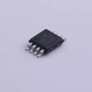
Image for reference only

Manufacturer Part:

CY2304SXI-1T

Package:

SOIC-8 (150-mil)

Brand:

Product Categories:

Quality Commitment

Shipping & Payment

Service & Packaging

Product Manual

Description

Product Overview

The CY2304SXI-1T is a 3.3V zero-delay clock buffer from Infineon Technologies (formerly Cypress Semiconductor) featuring an on-chip PLL that locks to the input reference and provides four low-skew outputs. Operating from 10 MHz to 133 MHz, it delivers less than 250 ps input-output skew and less than 200 ps output-to-output skew in an 8-pin SOIC package with industrial temperature range.

Key Specifications

  • Supply Voltage: 3.0V ~ 3.6V (3.3V nominal)
  • Input Frequency Range: 10 MHz ~ 133 MHz
  • Output Configuration: 1:4 (2 banks of 2 outputs each)
  • Input-to-Output Skew: < 250 ps
  • Output-to-Output Skew: < 200 ps
  • Cycle-to-Cycle Jitter: 90 ps typical at 66 MHz, 15 pF
  • Inter-Device Skew: < 500 ps
  • Configuration: CY2304-1 (all outputs = reference frequency)
  • Power-Down Current: < 25 µA (no REF input)
  • Operating Temperature: -40°C ~ +85°C (I suffix)
  • Package: SOIC-8 (150-mil)
  • REF Input: 5V tolerant

Features

  • Zero input-output propagation delay (adjustable via FBK loading)
  • On-chip PLL with external feedback for skew control
  • Low-skew, low-jitter clock distribution
  • Multiple output bank configurations (CY2304-1 and -2)
  • Power-down mode when REF input is absent
  • 5V tolerant reference input
  • Space-saving 8-pin SOIC package

Applications

  • PC and workstation clock distribution
  • Data communication equipment
  • Telecom systems
  • High-performance digital logic
  • PCI-X clock buffering
Product Introduction: CY2304SXI-1T Product Introduction

The CY2304SXI-1T from Infineon Technologies is a 3.3V zero-delay buffer designed for high-speed clock distribution in PC, workstation, datacom, and telecom applications. The on-chip phase-locked loop (PLL) locks to an input reference clock and generates four buffered outputs with guaranteed input-to-output skew below 250 ps and output-to-output skew below 200 ps. The feedback mechanism allows the user to adjust the input-output delay by varying the capacitive load on the FBK pin. In the CY2304-1 configuration, all outputs equal the reference frequency. The device enters power-down mode (< 25 µA) when no rising edges are detected on the REF input.

Working Principle: CY2304SXI-1T Working Principle

The CY2304SXI-1T uses a phase-locked loop (PLL) to achieve zero propagation delay between the reference input and the clock outputs. The REF pin receives the input clock, which drives the PLL’s phase detector. The PLL feedback is taken from one of the outputs (via the FBK pin), creating a closed loop that aligns the output phase with the input. By adjusting the capacitive load on the feedback path relative to the other outputs, the user can fine-tune the input-output delay for precise timing alignment. The four outputs are organized as two banks (Bank A: CLKA1, CLKA2; Bank B: CLKB1, CLKB2), each with matched propagation delays for minimal output-to-output skew. When REF stops toggling, the PLL powers down and all outputs are three-stated.

Pin Description: CY2304SXI-1T Pin Definition and Functions
Pin Name Function
1 REF Reference clock input (5V tolerant, weak pull-down)
2 CLKA1 Clock output, Bank A (weak pull-down)
3 CLKA2 Clock output, Bank A (weak pull-down)
4 GND Ground
5 CLKB1 Clock output, Bank B (weak pull-down)
6 CLKB2 Clock output, Bank B (weak pull-down)
7 VDD 3.3V power supply
8 FBK PLL feedback input
Application Scenarios: In which products and applications is CY2304SXI-1T used

The CY2304SXI-1T is used in high-performance computing platforms where precise clock distribution is critical for system timing margins. In PCI-X systems, it distributes a 66 MHz or 100 MHz clock to multiple card slots with guaranteed skew specifications. For networking equipment, it buffers reference clocks to multiple PHY devices and MAC controllers. The zero-delay feature is essential in synchronous digital systems where clock arrival time must be deterministic across all loads. Multiple CY2304 devices can share the same input clock with inter-device skew below 500 ps, enabling large clock trees.

Alternative Models: What chips are recommended as replacements for CY2304SXI-1T
Model Manufacturer Key Difference
CY2304SXI-2T Infineon Configurable output frequencies (1x, 2x, 0.5x)
CY2308SCI-1T Infineon 8-output version, 16-pin SOIC
PI49CTx02 Diodes Inc Pin-compatible alternative

Recommend Parts

TMP275AIDR

0.5C I2C temp sensor, 12-bit, 2.7-5.5V, alert output, 8-SOIC

Brand: TI

Package: 8-SOIC (4.90 x 3.91 x 1.50 mm)

IN STOCK: 3681pcs

Cargo cycle: 3-7 Days

The minimum order is 1

IL485E

NVE IL485E IsoLoop isolated RS-485 transceiver, 2.5kVrms isolation, 35Mbps, 16-SOIC WB

Brand: nve

Package: SOIC-16 WB

IN STOCK: 5280pcs

Cargo cycle: 3-7 Days

The minimum order is 1

IRFS4227TRLPBF

IRFS4227TRLPBF – 200V N-Channel HEXFET PDP Switch Power MOSFET, 26 mΩ RDS(on), D2PAK (TO-263)

Brand: infineon

Package: D2PAK (TO-263)

IN STOCK: 4334pcs

Cargo cycle: 3-7 Days

The minimum order is 1

CD4070BM96

Quad 2-input XOR gate, 3-18V CMOS, 65ns at 10V, SOIC-14

Brand: TI

Package: SOIC-14 (8.75 x 3.9 x 1.5mm)

IN STOCK: 4245pcs

Cargo cycle: 3-7 Days

The minimum order is 1

AB1526

Bluetooth 5.0 Dual Mode Audio SoC, TWS, AAC, Dual-mic ENC, Integrated Charger, BGA

Brand: airoha

Package: BGA

IN STOCK: 25000pcs

Cargo cycle: 3-7 Days

The minimum order is 1

LP2980IM5-5.0

50mA micropower ultra-low-dropout regulator, 5V, SOT-23-5

Brand: TI

Package: SOT-23-5 (2.9 x 1.6 x 1.1 mm)

IN STOCK: 2557pcs

Cargo cycle: 3-7 Days

The minimum order is 1