
Opens in a new tab

AD650JNZ

V/F and F/V converter, 1MHz FS, 0.07% linearity, ±15V, PDIP-14

1897

Effective Inventory

Image for reference only

Manufacturer Part:

AD650JNZ

Package:

PDIP-14 (7.62 x 19.3 mm)

Brand:

Quality Commitment

Shipping & Payment

Service & Packaging

Product Manual

Other recommendations you may be interested in.

Description

Product Overview

The AD650JNZ from Analog Devices is a voltage-to-frequency (V/F) and frequency-to-voltage (F/V) converter that provides high-accuracy analog-to-digital conversion with a linear transfer function. Operating at up to 1MHz full-scale frequency from ±15V supplies, it offers 0.07% max linearity error in a PDIP-14 package.

Key Specifications

Function V/F and F/V Converter
Full-Scale Frequency Up to 1 MHz
Linearity Error 0.07% max (100kHz FS)
Supply Voltage ±5V to ±18V
Input Voltage Range 0 to 10V (unipolar), ±10V (bipolar)
Drift 15 ppm/°C (gain)
Package PDIP-14
Operating Temperature 0°C to +70°C (J grade)

Features

  • Voltage-to-frequency and frequency-to-voltage conversion in one device
  • High linearity: 0.07% max at 100kHz full scale
  • Wide dynamic range with monotonic transfer characteristic
  • Up to 1MHz full-scale output frequency
  • Bipolar input capability for AC signal conversion
  • Open-collector frequency output with TTL/CMOS compatibility

Applications

  • High-resolution analog-to-digital conversion using counter-based methods
  • Long-distance analog signal transmission over digital links
  • Isolated data acquisition with optocoupler-compatible output
  • Motor speed measurement and tachometer applications
  • Process control and instrumentation signal conditioning
Product Introduction: AD650JNZ Product Introduction

The AD650JNZ from Analog Devices is a versatile voltage-to-frequency and frequency-to-voltage converter that provides high-accuracy signal conversion with a linear, monotonic transfer characteristic. As a V/F converter, it transforms an analog input voltage into a proportional output frequency with linearity error as low as 0.07% at 100kHz full scale. As an F/V converter, it performs the inverse function. The device can operate at full-scale frequencies up to 1MHz and accepts both unipolar (0-10V) and bipolar (±10V) input ranges. The open-collector frequency output is compatible with TTL, CMOS, and optocoupler inputs, making it ideal for applications requiring galvanic isolation or long-distance analog signal transmission over digital links.

Working Principle: AD650JNZ Working Principle

The AD650 operates using a charge-balance architecture for V/F conversion. (1) In V/F mode, the input voltage drives a current (proportional to VIN) into the integrator op-amp, which produces a ramping output voltage. When the integrator output crosses the comparator threshold, a one-shot timer is triggered, activating the precision current source that discharges the integrator by a fixed amount of charge. The one-shot duration is precisely controlled by an external capacitor. (2) The output pulse frequency is proportional to the input voltage because the rate at which charge-balancing pulses occur equals the rate at which input current charges the integrator. Each output pulse removes a fixed quantum of charge (IREF x tOS), so the pulse frequency FOUT = VIN / (IREF x tOS x RIN). (3) In F/V mode, the input frequency triggers the one-shot timer, which generates fixed-width current pulses that are integrated by an external RC network to produce a DC output voltage proportional to the input frequency.

Pin Description: AD650JNZ Pin Definition and Functions
Pin Name Function
1 VOUT Frequency output (open collector)
2 COMPARATOR INPUT Comparator threshold input
3 ANALOG GND Analog ground
4 +IN Non-inverting input
5 -IN Inverting input (signal input)
6 V+ Positive supply (+15V)
7 COS1 One-shot timing capacitor
8 COS2 One-shot timing capacitor
9 D1 Current source digital control
10 D2 Current source digital control
11 CINT Integrator capacitor connection
12 RIN Input resistor connection
13 V- Negative supply (-15V)
14 DIGITAL GND Digital ground
Application Scenarios: In which products and applications is AD650JNZ used
  • High-resolution ADC using V/F conversion with counter-based digital measurement
  • Isolated analog signal transmission over optical fiber or transformer links
  • Motor speed tachometer frequency-to-voltage conversion
  • Process control 4-20mA to frequency conversion for long-distance transmission
  • Precision integrator applications requiring charge-balance architecture
Alternative Models: What chips are recommended as replacements for AD650JNZ
Model Manufacturer Key Difference
AD650KNZ Analog Devices Industrial temp, 0.02% linearity
AD650SD Analog Devices Military temp, 0.02% linearity
VFC32KU TI V/F converter, 500kHz, SOIC-14
LM331 TI 100kHz V/F, lower performance
ADVFC32AH Analog Devices 500kHz V/F, hermetic DIP

Recommend Parts

IRFS4310ZTRLPBF

IRFS4310ZTRLPBF – 100V N-Channel HEXFET Power MOSFET, 7 mΩ RDS(on), D2PAK (TO-263AB)

Brand: infineon

Package: D2PAK (TO-263AB)

IN STOCK: 11137pcs

Cargo cycle: 3-7 Days

The minimum order is 1

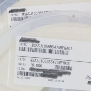
MSASJ105BB5475MFNA01

4.7uF 6.3V X5R MLCC, 0402, Taiyo Yuden

Brand: gigadevice

Package: 0402 (1005 Metric, 1.0 x 0.5 x 0.5 mm)

IN STOCK: 9701pcs

Cargo cycle: 3-7 Days

The minimum order is 1

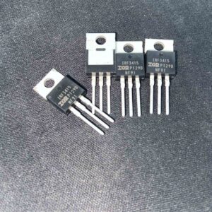
IRF3415PBF

150V N-channel power MOSFET, 43A, 41mΩ RDS(on), TO-220AB package

Brand: infineon

Package: TO-220AB

IN STOCK: 2940pcs

Cargo cycle: 3-7 Days

The minimum order is 1

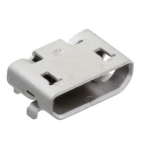
105017-1001

USB Type-C receptacle connector, 24-pin, SMD

Brand: Amphenol

Package: SMD (8.9 x 7.3 x 3.2 mm, right angle)

IN STOCK: 5335pcs

Cargo cycle: 3-7 Days

The minimum order is 1

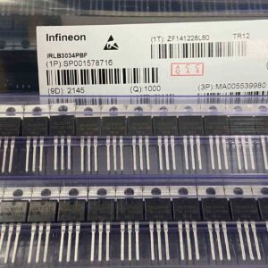
IRLB3034PBF

IRLB3034PBF – 40V N-Channel StrongIRFET Power MOSFET (Logic Level), 1.7 mΩ (max) @ 10V; 2.0 mΩ @ 4.5V RDS(on), TO-220AB

Brand: infineon

Package: TO-220AB

IN STOCK: 9724pcs

Cargo cycle: 3-7 Days

The minimum order is 1

XC6SLX75-2FGG484I

Spartan-6 LX75 FPGA, 74637 logic cells, 132 DSP, 3096KB BRAM, 408 I/O, FBGA-484 23x23mm, -2 speed, industrial -40~100C, AMD Xilinx

Brand: xilinx

Package: FGG484 (484-ball fine-pitch BGA, 23x23mm body, 1.0mm ball pitch, 22×22 ball array, 6 I/O banks, lead-free)

IN STOCK: 890pcs

Cargo cycle: 3-7 Days

The minimum order is 1