Opens in a new tab

TPS61230DRC

5A sync boost converter, 2.3-5.5V in, 2.5-5.5V adj out, 2MHz, VSON-10

5300

Effective Inventory

Image for reference only

Manufacturer Part:

TPS61230DRC

Package:

VSON-10 DRC (3.0 x 3.0 x 0.9mm, 0.5mm pitch with thermal pad)

Brand:

Quality Commitment

Shipping & Payment

Service & Packaging

Product Manual

Description

Product Overview

The TPS61230DRC is a 5A synchronous boost converter from Texas Instruments with 2.3-5.5V input, adjustable 2.5-5.5V output, 2MHz switching, and power save mode in a VSON-10 package.

Key Specifications

Input Voltage Range 2.3V to 5.5V
Output Voltage 2.5V to 5.5V (adjustable via resistor divider)
Output Current Up to 2.1A at 5V from 3.3V input
Internal Switch Current 5A (integrated N-channel MOSFETs)
Switching Frequency 2MHz typical
Efficiency Up to 96%
Quiescent Current 60µA (power save mode)
Shutdown Current 1.5µA typical
Synchronous Rectification Yes (integrated)
Operating Temperature -40°C to +125°C
Package VSON-10 (3 x 3 x 0.9mm, DRC)

Features

  • High efficiency synchronous boost up to 96%
  • 5A integrated switch for high output power
  • 2MHz switching enables small inductors and capacitors
  • Power save mode for light-load efficiency
  • Load disconnect during shutdown (1.5µA IQ)
  • Adjustable EN threshold with hysteresis
  • Output overvoltage protection
  • Power good output for system sequencing
  • Programmable soft start

Applications

  • Li-Ion to 5V USB power conversion
  • Single-cell battery boost for 3.3V or 5V rails
  • Portable medical and industrial devices
  • USB power bank circuits
  • White LED driver for backlight
Product Introduction: TPS61230DRC Product Introduction

The TPS61230DRC from Texas Instruments is a high-efficiency synchronous boost converter with an integrated 5A switch, capable of delivering up to 2.1A at 5V from a 3.3V input. The 2MHz switching frequency allows the use of small inductors (1.0-2.2µH) and ceramic capacitors, minimizing solution size. The quasi-constant on-time valley current mode control provides fast transient response. During light loads, the device automatically enters power save mode (PSM) with 60µA quiescent current for maximum efficiency. In shutdown, the load is completely disconnected from the input with only 1.5µA input current. The adjustable output voltage (2.5V to 5.5V) is set via an external resistor divider. Additional features include output overvoltage protection, programmable soft start, thermal shutdown, and a power good output. The VSON-10 package (3 x 3mm) provides excellent thermal performance with a bottom-side thermal pad.

Working Principle: TPS61230DRC Working Principle

The TPS61230DRC uses a quasi-constant on-time valley current mode control scheme for boost regulation. During each switching cycle, the high-side NMOS switch turns on and current builds in the inductor. The on-time is adjusted quasi-constantly based on input and output voltage to maintain approximately 2MHz switching frequency. When the switch turns off, the synchronous rectifier (low-side NMOS) turns on and the inductor current flows to the output capacitor and load. The valley current mode compares the inductor current (sensed through the switch) with the error amplifier output; when the inductor valley current drops below the threshold, a new on-time begins. In power save mode (PSM), the device operates in PFM (pulse frequency modulation) mode at light loads: the switch operates with a fixed on-time and skips pulses, reducing switching losses and maintaining efficiency above 80% even at 1mA load. The EN pin has an adjustable threshold set by external resistors, allowing the system to power up only when the input voltage exceeds a desired level. The power good (PG) output goes high when the output reaches 90% of the target voltage, enabling sequenced power-up of downstream loads. The output overvoltage protection (OVP) disables switching if the output exceeds the OVP threshold, protecting downstream components. The soft start ramp limits inrush current during startup.

Pin Description: TPS61230DRC Pin Definition and Functions
Pin Name Type Description
1 SW Power Switch node (connect to inductor)
2 SW Power Switch node (connect to inductor)
3 VIN Power Input supply (2.3-5.5V)
4 EN Input Enable (high=on, adjustable threshold)
5 SS Analog Soft start (connect capacitor to GND)
6 FB Input Feedback (connect resistor divider from VOUT)
7 PG Output Power good output (open-drain)
8 VOUT Power Boost output (2.5-5.5V)
9 GND Power Ground
10 GND Power Ground
Pad PowerPAD Power Thermal pad (connect to GND plane)

TPS61230DRC uses the VSON-10 (3x3mm, DRC) surface-mount package from TI: Pins 1,2 = VOUT, Pin 3 = PG (Power Good, open-drain), Pin 4 = FB (Feedback, connect to VOUT directly for 5V fixed), Pin 5 = EN (Enable, active-high), Pin 6 = GND, Pins 7,8 = SW (switch node, connect inductor), Pins 9,10 = VIN, Exposed Pad = GND. Dual VOUT and SW pins distribute high current and reduce parasitic inductance. The PG pin pulls LOW when output is below 90% of regulation. The EN pin has a precision threshold (1.2V typ) for programmable UVLO using external resistors. The exposed pad must be soldered to a ground plane with thermal vias for proper heat dissipation. Place the input capacitor within 2mm of VIN pins.

Application Scenarios: In which products and applications is TPS61230DRC used
  • USB Power Banks: Boosts single Li-Ion (3.0-4.2V) to 5V/2.1A for USB output; 96% efficiency maximizes battery life
  • Battery to 3.3V: Boosts single-cell Li-Ion to regulated 3.3V for MCU and sensor rails in portable devices
  • Portable Medical: Load disconnect in shutdown (1.5µA) and PSM at light loads extend battery operation
  • White LED Backlight: Adjustable output drives series LED strings; PG output sequences LED driver enable
  • Industrial Sensors: 2MHz and small VSON package enable compact boost regulator near sensor modules
Alternative Models: What chips are recommended as replacements for TPS61230DRC
Model Manufacturer Key Difference Package Specs
TPS61230DRCT TI Tape & reel version – –
TPS61232DRC TI Fixed 5V output version – –
TPS61088RHLT TI 10A, 2.2-5.5V, VQFN-12, higher power – –
LTC3426ETS#TRPBF ADI 3A, 1.8-5.5V, 2MHz, TSOT-23-8 – –
MAX17050ETD+T Maxim/ADI 5A, 0.7-5.5V, TDFN-14 – –

TPS61230DRC is a 5A synchronous boost converter from TI in VSON-10 (3x3mm). The TPS61235P provides 8A switch current for higher power. The TPS61232 offers adjustable output version. The LTC3426 from ADI provides 3A boost with 1.5MHz switching. The MT3608 from Aerosemi offers 2A boost at lower cost in SOT-23-6. The MP3425 from MPS provides 6A boost with 500kHz switching. The MAX17017 from ADI/Maxim offers 10A boost for battery-powered systems. For lower current, TPS61021 provides 1.5A in smaller VFBGA-6.

Recommend Parts

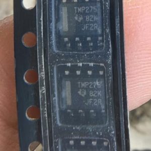
TMP275AIDR

0.5C I2C temp sensor, 12-bit, 2.7-5.5V, alert output, 8-SOIC

Brand: TI

Package: 8-SOIC (4.90 x 3.91 x 1.50 mm)

IN STOCK: 3681pcs

Cargo cycle: 3-7 Days

The minimum order is 1

IL485E

NVE IL485E IsoLoop isolated RS-485 transceiver, 2.5kVrms isolation, 35Mbps, 16-SOIC WB

Brand: nve

Package: SOIC-16 WB

IN STOCK: 5280pcs

Cargo cycle: 3-7 Days

The minimum order is 1

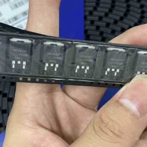
IRFS4227TRLPBF

IRFS4227TRLPBF – 200V N-Channel HEXFET PDP Switch Power MOSFET, 26 mΩ RDS(on), D2PAK (TO-263)

Brand: infineon

Package: D2PAK (TO-263)

IN STOCK: 4334pcs

Cargo cycle: 3-7 Days

The minimum order is 1

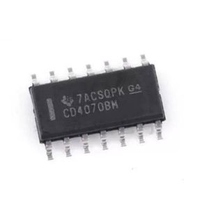
CD4070BM96

Quad 2-input XOR gate, 3-18V CMOS, 65ns at 10V, SOIC-14

Brand: TI

Package: SOIC-14 (8.75 x 3.9 x 1.5mm)

IN STOCK: 4245pcs

Cargo cycle: 3-7 Days

The minimum order is 1

AB1526

Bluetooth 5.0 Dual Mode Audio SoC, TWS, AAC, Dual-mic ENC, Integrated Charger, BGA

Brand: airoha

Package: BGA

IN STOCK: 25000pcs

Cargo cycle: 3-7 Days

The minimum order is 1

LP2980IM5-5.0

50mA micropower ultra-low-dropout regulator, 5V, SOT-23-5

Brand: TI

Package: SOT-23-5 (2.9 x 1.6 x 1.1 mm)

IN STOCK: 2557pcs

Cargo cycle: 3-7 Days

The minimum order is 1