Opens in a new tab

LTC2852IMS

3.3V full-duplex RS-485, 20Mbps, ±15kV HBM, 5µA shutdown, MSOP-10

4200

Effective Inventory

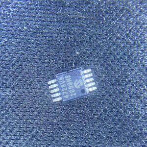
Image for reference only

Manufacturer Part:

LTC2852IMS

Package:

MSOP-10 (3.0 x 3.0 x 0.9mm, 0.5mm pitch)

Brand:

Quality Commitment

Shipping & Payment

Service & Packaging

Product Manual

Other recommendations you may be interested in.

Description

Product Overview

The LTC2852IMS is a 3.3V full-duplex RS-485/RS-422 transceiver from Analog Devices with 20Mbps data rate, driver/receiver enables, ±15kV HBM ESD, and 5µA shutdown in an MSOP-10 package.

Key Specifications

Supply Voltage 3.3V (3.0V to 3.6V)
Data Rate 20Mbps max
Duplex Full (separate TX and RX)
ESD Protection (HBM) ±15kV on bus pins
Driver Output (VOD) 1.5V min into 54Ω differential load
Receiver Sensitivity ±200mV threshold
Failsafe Yes (high output on open/shorted inputs)
Nodes per Bus 256 (1/8 unit load, I-grade)
Shutdown Current 5µA max
Operating Current (RX mode) 370µA typical
Operating Temperature -40°C to +85°C (I-grade)
Package MSOP-10 (3 x 3mm)

Features

  • Full-duplex with separate driver and receiver enables (DE, RE)
  • 20Mbps data rate for high-speed communication
  • ±15kV HBM ESD protection on bus interface
  • Guaranteed failsafe receiver (high output on open/short bus)
  • 5µA micropower shutdown mode (DE=low, RE=high)
  • 370µA receive-mode current for low-power operation
  • Glitch-free driver outputs during power-up/down
  • Current-limited drivers and thermal shutdown protection

Applications

  • Low-power RS-485/RS-422 communication
  • Level translation between 3.3V logic and RS-485 bus
  • Backplane transceivers
  • Industrial networking
  • Battery-powered instrumentation
Product Introduction: LTC2852IMS Product Introduction

The LTC2852IMS from Analog Devices is a 3.3V full-duplex RS-485/RS-422 transceiver with driver enable (DE) and receiver enable (RE) pins for flexible bus control. It supports data rates up to 20Mbps with ±15kV HBM ESD protection on bus pins. The guaranteed failsafe receiver output goes high when the bus inputs are open or shorted, preventing undefined data. The 1/8 unit load allows up to 256 nodes on a single bus. The 5µA micropower shutdown mode is achieved by driving DE low and RE high, making it ideal for battery-powered applications. The driver outputs are glitch-free during power-up and power-down, preventing bus corruption in hot-plug systems. The MSOP-10 package (3 x 3mm) saves board space compared to SOIC packages.

Working Principle: LTC2852IMS Working Principle

The LTC2852IMS converts between 3.3V TTL/CMOS logic levels and RS-485 differential bus signals in full-duplex mode. The driver section takes the DI input and, when DE is high, drives the Y and Z outputs as a differential pair: DI high produces positive VOD (Y>Z), DI low produces negative VOD (Y<Z). When DE is low, both driver outputs are high-impedance. The receiver section continuously monitors the A-B differential voltage when RE is low; when |VA-VB| exceeds 200mV, the RO output reflects the polarity. The failsafe biasing ensures RO is high when VA-VB is between -200mV and +200mV (open or shorted bus). When RE is high, RO is high-impedance. The 5µA shutdown is a delayed micropower mode entered when DE is low and RE is high simultaneously; the device fully exits shutdown in approximately 50µs when either enable changes. The driver outputs are current-limited to ±250mA and protected by thermal shutdown that disables the driver at approximately 160°C junction temperature. The receiver has a 1/8 unit load input impedance, allowing 256 transceivers on one bus.

Pin Description: LTC2852IMS Pin Definition and Functions
Pin Name Type Description
1 RO Output Receiver data output (3-state when RE=high)
2 RE Input Receiver enable (active low)
3 DE Input Driver enable (active high)
4 DI Input Driver data input
5 GND1 Power Ground (logic side)
6 Y Output Driver non-inverting output
7 Z Output Driver inverting output
8 B Input Receiver inverting input (bus)
9 A Input Receiver non-inverting input (bus)
10 VCC Power Supply (3.0-3.6V)

LTC2852IMS uses the 10-lead MSOP (3x3mm) surface-mount package from Analog Devices: Pin 1 = RO (Receiver Output), Pin 2 = RE (Receiver Enable, active-low), Pin 3 = DE (Driver Enable, active-high), Pin 4 = DI (Driver Input), Pin 5 = GND, Pin 6 = Y (Driver Output, non-inverting), Pin 7 = Z (Driver Output, inverting), Pin 8 = B (Receiver Input, inverting), Pin 9 = A (Receiver Input, non-inverting), Pin 10 = VCC (3.0-3.6V). This is a full-duplex transceiver — driver and receiver operate simultaneously on separate bus pairs (Y/Z for transmit, A/B for receive). For half-duplex, short Y to A and Z to B. The MSOP-10 pinout is compatible with LTC2850/2851/2853 family devices.

Application Scenarios: In which products and applications is LTC2852IMS used
  • Low-Power Comm: 370µA RX mode and 5µA shutdown extend battery life in portable instrumentation and field devices
  • Backplane: Glitch-free power transitions prevent data corruption when cards are hot-plugged into live backplanes
  • Level Translation: 3.3V logic interface with ±7V common-mode RS-485 bus provides level isolation
  • Multi-Drop: 256-node capability with guaranteed failsafe allows large sensor networks without external bias resistors
  • Industrial: ±15kV HBM ESD and current-limited drivers survive harsh industrial environments with electrical noise
Alternative Models: What chips are recommended as replacements for LTC2852IMS
Model Manufacturer Key Difference Package Specs
LTC2852IS ADI Same in SOIC-14 package – –
LTC2852HMS ADI High temp (-40°C to +125°C), MSOP-10 – –
SN65HVD73DGKR TI 3.3V full-duplex, 20Mbps, with enables, VSSOP-8 – –
ISL3179EFVZ-T7 Renesas 3.3V full-duplex, 20Mbps, TSSOP-14 – –
MAX3485ECSA+ Maxim/ADI 3.3V half-duplex, 12Mbps, SOIC-8 – –

LTC2852IMS is a 3.3V 20Mbps RS485/RS422 full-duplex transceiver from ADI in MSOP-10. The LTC2851 provides half-duplex operation in MSOP-8. The LTC2854 adds auto-direction control for simplified bus management. The SN65HVD74DGKR from TI provides 3.3V full-duplex with ±30kV ESD. The ADM3485ARZ from ADI offers 3.3V half-duplex in SOIC-8. The THVD1550 from TI provides 50Mbps in VSSOP-8. For 5V operation, LTC485 provides 250kbps half-duplex in SOIC-8.

Recommend Parts

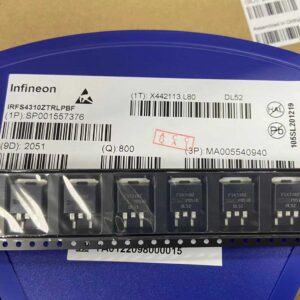
IRFS4310ZTRLPBF

IRFS4310ZTRLPBF – 100V N-Channel HEXFET Power MOSFET, 7 mΩ RDS(on), D2PAK (TO-263AB)

Brand: infineon

Package: D2PAK (TO-263AB)

IN STOCK: 11137pcs

Cargo cycle: 3-7 Days

The minimum order is 1

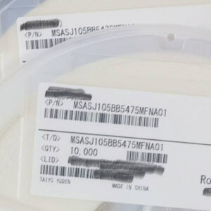
MSASJ105BB5475MFNA01

4.7uF 6.3V X5R MLCC, 0402, Taiyo Yuden

Brand: gigadevice

Package: 0402 (1005 Metric, 1.0 x 0.5 x 0.5 mm)

IN STOCK: 9701pcs

Cargo cycle: 3-7 Days

The minimum order is 1

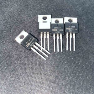
IRF3415PBF

150V N-channel power MOSFET, 43A, 41mΩ RDS(on), TO-220AB package

Brand: infineon

Package: TO-220AB

IN STOCK: 2940pcs

Cargo cycle: 3-7 Days

The minimum order is 1

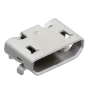
105017-1001

USB Type-C receptacle connector, 24-pin, SMD

Brand: Amphenol

Package: SMD (8.9 x 7.3 x 3.2 mm, right angle)

IN STOCK: 5335pcs

Cargo cycle: 3-7 Days

The minimum order is 1

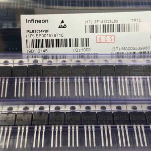
IRLB3034PBF

IRLB3034PBF – 40V N-Channel StrongIRFET Power MOSFET (Logic Level), 1.7 mΩ (max) @ 10V; 2.0 mΩ @ 4.5V RDS(on), TO-220AB

Brand: infineon

Package: TO-220AB

IN STOCK: 9724pcs

Cargo cycle: 3-7 Days

The minimum order is 1

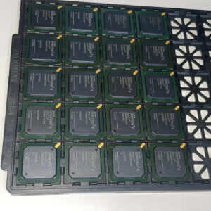
XC6SLX75-2FGG484I

Spartan-6 LX75 FPGA, 74637 logic cells, 132 DSP, 3096KB BRAM, 408 I/O, FBGA-484 23x23mm, -2 speed, industrial -40~100C, AMD Xilinx

Brand: xilinx

Package: FGG484 (484-ball fine-pitch BGA, 23x23mm body, 1.0mm ball pitch, 22×22 ball array, 6 I/O banks, lead-free)

IN STOCK: 890pcs

Cargo cycle: 3-7 Days

The minimum order is 1