Opens in a new tab

SN74LVC2G34DCKR

Dual buffer gate, 1.65-5.5V, +/-24mA drive, 5.5V-tolerant input, SC70-6, level shift

3679

Effective Inventory

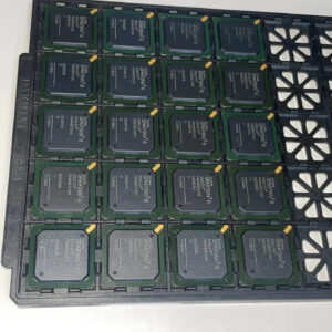
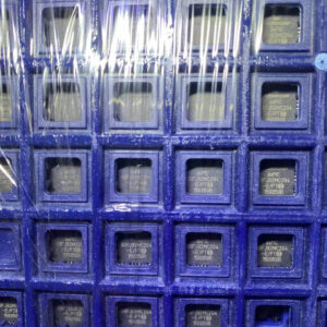
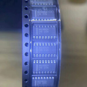
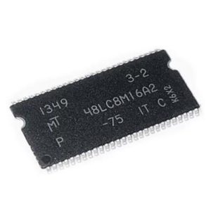
Image for reference only

Manufacturer Part:

SN74LVC2G34DCKR

Package:

SC70-6 / SOT-363 (2.0 x 1.25 x 0.9 mm)

Brand:

Quality Commitment

Shipping & Payment

Service & Packaging

Product Manual

Other recommendations you may be interested in.

Description

Product Overview

The SN74LVC2G34DCKR from Texas Instruments is a dual buffer gate designed for 1.65V to 5.5V VCC operation in a 6-pin SC70 (DCK) package. Performing the Boolean function Y = A in positive logic, it supports 5.5V-tolerant inputs for voltage translation, provides +/-24 mA output drive at 3.3V, and features Ioff circuitry for partial-power-down protection.

Key Specifications

Function Dual Buffer (non-inverting)
Supply Voltage 1.65V to 5.5V
Input Voltage Tolerance Up to 5.5V
Output Drive +/-24 mA @ 3.3V
Propagation Delay 4.1 ns max @ 3.3V
Quiescent Current 10 uA max
Ioff Support Yes (partial-power-down)
ESD Protection 2000V HBM, 1000V CDM
Operating Temperature -40°C to +125°C
Package SC70-6 (DCK) (2.0 x 1.25 x 0.9 mm)

Features

  • NanoFree package technology for minimal footprint
  • 5.5V-tolerant inputs enable down-translation
  • Low power consumption: 10 uA max ICC
  • +/-24 mA output drive at 3.3V
  • Ioff supports live insertion and back-drive protection
  • Latch-up exceeds 100 mA per JESD78 Class II

Applications

  • Level translation between voltage domains
  • Signal buffering and fanout enhancement
  • AV receivers and home theater systems
  • Portable audio and MP3 players
  • Solid-state drives and embedded PCs
Product Introduction: SN74LVC2G34DCKR Product Introduction

The Texas Instruments SN74LVC2G34DCKR is a dual non-inverting buffer gate from the 74LVC family, designed for 1.65V to 5.5V VCC operation in a miniature 6-pin SC70 (DCK) package using NanoFree packaging technology. It performs the Boolean function Y = A, providing signal buffering with 5.5V-tolerant inputs that accept voltages higher than the supply rail, enabling down-translation from 5V or 3.3V logic to lower voltage domains. The device delivers +/-24 mA output drive at 3.3V with a maximum propagation delay of 4.1 ns. The Ioff feature allows the inputs and outputs to be valid when VCC is 0V, supporting live insertion, partial-power-down mode, and back-drive protection in mixed-voltage systems.

Working Principle: SN74LVC2G34DCKR Working Principle

The SN74LVC2G34DCKR consists of two independent non-inverting buffer channels. Each channel accepts an input signal (A) and produces an output (Y) that replicates the input logic level. The output stage uses CMOS push-pull transistors capable of sourcing or sinking 24 mA at 3.3V, providing sufficient drive for multiple downstream loads or transmission lines. The input stage is designed to tolerate voltages up to 5.5V regardless of VCC, allowing the device to translate a higher-voltage input signal down to the VCC level at the output. The Ioff circuit disconnects the output stage when VCC is 0V, preventing parasitic current flow from the input through internal ESD diodes to the unpowered supply rail. This enables safe use in hot-swap and partial-power-down systems where some signals may be active while the buffer supply is off.

Pin Description: SN74LVC2G34DCKR Pin Definition and Functions
Pin Name Description
1 1A Channel 1 Input
2 GND Ground
3 2A Channel 2 Input
4 2Y Channel 2 Output
5 VCC Supply Voltage (1.65-5.5V)
6 1Y Channel 1 Output
Application Scenarios: In which products and applications is SN74LVC2G34DCKR used
  • Level Translation: Down-translating 5V logic signals to 3.3V or 1.8V domains using 5.5V-tolerant inputs without external level shifter ICs
  • Signal Buffering: Increasing fanout capability of microcontroller GPIO pins by isolating the source from capacitive load effects
  • Hot-Swap Systems: Ioff protection allows safe signal routing in blade servers and modular systems where cards may be inserted with power off
  • Audio/Video Equipment: Signal integrity buffering in AV receivers and Blu-ray players with 125°C operating range
  • SSD Controllers: Fast 4.1 ns propagation for NAND Flash interface signal conditioning in enterprise and client SSDs
Alternative Models: What chips are recommended as replacements for SN74LVC2G34DCKR
Model Brand Channels VCC (V) Package
SN74LVC2G34DBVR TI 2 1.65-5.5 SOT-23-6
SN74LVC1G34DCKR TI 1 1.65-5.5 SC70-5
NC7WZ16P6X onsemi 2 1.65-5.5 SC70-6
74LVC2G34GW NXP 2 1.65-5.5 TSSOP-6
SN74LVC2G125DCKR TI 2 (3-state) 1.65-5.5 SC70-6

Recommend Parts

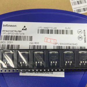
IRFS4310ZTRLPBF

IRFS4310ZTRLPBF – 100V N-Channel HEXFET Power MOSFET, 7 mΩ RDS(on), D2PAK (TO-263AB)

Brand: infineon

Package: D2PAK (TO-263AB)

IN STOCK: 11137pcs

Cargo cycle: 3-7 Days

The minimum order is 1

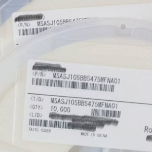
MSASJ105BB5475MFNA01

4.7uF 6.3V X5R MLCC, 0402, Taiyo Yuden

Brand: gigadevice

Package: 0402 (1005 Metric, 1.0 x 0.5 x 0.5 mm)

IN STOCK: 9701pcs

Cargo cycle: 3-7 Days

The minimum order is 1

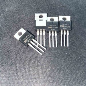
IRF3415PBF

150V N-channel power MOSFET, 43A, 41mΩ RDS(on), TO-220AB package

Brand: infineon

Package: TO-220AB

IN STOCK: 2940pcs

Cargo cycle: 3-7 Days

The minimum order is 1

105017-1001

USB Type-C receptacle connector, 24-pin, SMD

Brand: Amphenol

Package: SMD (8.9 x 7.3 x 3.2 mm, right angle)

IN STOCK: 5335pcs

Cargo cycle: 3-7 Days

The minimum order is 1

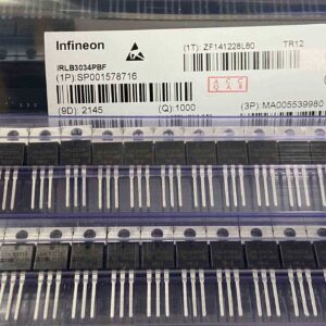
IRLB3034PBF

IRLB3034PBF – 40V N-Channel StrongIRFET Power MOSFET (Logic Level), 1.7 mΩ (max) @ 10V; 2.0 mΩ @ 4.5V RDS(on), TO-220AB

Brand: infineon

Package: TO-220AB

IN STOCK: 9724pcs

Cargo cycle: 3-7 Days

The minimum order is 1

XC6SLX75-2FGG484I

Spartan-6 LX75 FPGA, 74637 logic cells, 132 DSP, 3096KB BRAM, 408 I/O, FBGA-484 23x23mm, -2 speed, industrial -40~100C, AMD Xilinx

Brand: xilinx

Package: FGG484 (484-ball fine-pitch BGA, 23x23mm body, 1.0mm ball pitch, 22×22 ball array, 6 I/O banks, lead-free)

IN STOCK: 890pcs

Cargo cycle: 3-7 Days

The minimum order is 1