Opens in a new tab

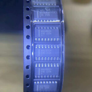
SN74LVC74ADR

Dual D FF, preset/clear, 5.5V input, SOIC-14

8500

Effective Inventory

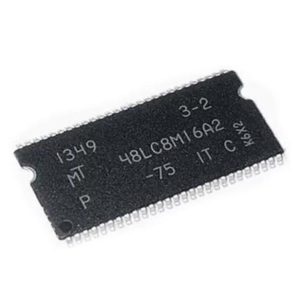
Image for reference only

Manufacturer Part:

SN74LVC74ADR

Package:

14-Pin SOIC (8.65 x 3.9 x 1.5 mm)

Brand:

Quality Commitment

Shipping & Payment

Service & Packaging

Product Manual

Other recommendations you may be interested in.

Description

Product Overview

The SN74LVC74ADR is a Texas Instruments dual D-type positive-edge-triggered flip-flop with preset, clear, and 3-state outputs. 1.65-3.6V supply, 5.5V tolerant inputs. Packaged in SOIC-14, -40C to +125C.

Key Specifications

Channels 2 (dual)
Type D flip-flop, edge-triggered
Supply 1.65 V to 3.6 V
fmax >200 MHz at 3.3V
Input Tolerance 5.5 V
Package SOIC-14

Features

  • Dual D flip-flop with preset/clear
  • Positive-edge-triggered clock
  • 1.65V to 3.6V supply
  • 5.5V tolerant inputs
  • >200MHz max clock frequency
  • Complementary Q and Q-bar outputs
  • Ioff partial-power-down support

Applications

  • Clock division and sync
  • Data latch and pipeline
  • Control state machine
  • Level translation
Product Introduction: SN74LVC74ADR Product Introduction

The SN74LVC74ADR is a Texas Instruments dual D-type positive-edge-triggered flip-flop with asynchronous preset (PRE) and clear (CLR) inputs in a 14-pin SOIC package. Each flip-flop captures the D input on the rising edge of the clock (CLK) and presents it at the Q output, with the complementary Q-bar output always opposite. The asynchronous PRE (active low) sets Q high regardless of clock, and CLR (active low) resets Q low. Both PRE and CLR override the clocked operation, providing flexible initialization and fault handling. The 1.65V to 3.6V supply range supports 1.8V, 2.5V, and 3.3V logic systems. The 5.5V input tolerance allows direct interfacing with 5V logic devices, enabling 5V-to-3.3V level translation. The >200MHz maximum clock frequency at 3.3V supports high-speed clock division and data pipeline applications. The Ioff feature disables the output circuitry during partial power-down, preventing backflow current. The LVC architecture provides low static power consumption with high output drive (24mA at 3.3V). Packaged in SOIC-14 rated for -40C to +125C.

Working Principle: SN74LVC74ADR Working Principle

The SN74LVC74A contains two independent D flip-flops, each implemented as a master-slave latch. On the rising edge of CLK, the master latch opens and captures the D input value while the slave latch holds the previous Q output. After the clock transition, the master closes and the slave opens, transferring the new value to the Q output. This edge-triggered behavior prevents transparent latching that could cause race conditions. The asynchronous PRE input asserts Q=1 and Q-bar=0 by directly setting the slave latch, overriding the clocked D input. Similarly, CLR asserts Q=0 and Q-bar=1 by directly resetting the slave latch. If both PRE and CLR are asserted simultaneously, both Q and Q-bar go high (invalid state), which resolves when either preset or clear is released. The input clamp diodes protect against overshoot and allow 5.5V inputs when VCC is 3.3V. The output stage uses a push-pull CMOS driver sized for 24mA symmetric drive.

Pin Description: SN74LVC74ADR Pin Definition and Functions
Pin Mnemonic Description
1 1CLR Clear 1 (active low)
2 1D Data input 1
3 1CLK Clock 1 (rising edge)
4 1PRE Preset 1 (active low)
5 1Q Output 1
6 1Q-bar Complementary output 1
7 GND Ground
8 2Q-bar Complementary output 2
9 2Q Output 2
10 2PRE Preset 2 (active low)
11 2CLK Clock 2 (rising edge)
12 2D Data input 2
13 2CLR Clear 2 (active low)
14 VCC Supply (1.65-3.6V)
Application Scenarios: In which products and applications is SN74LVC74ADR used
  • Clock division by 2 with D tied to Q-bar for toggle flip-flop operation at >200MHz
  • Data pipeline stage with edge-triggered capture and preset/clear for initialization
  • Control state machine element with asynchronous clear for fault reset
  • 5V-to-3.3V level translation with 5.5V tolerant inputs and clocked data capture
Alternative Models: What chips are recommended as replacements for SN74LVC74ADR
Model Manufacturer Key Difference
SN74LVC74APWR TI TSSOP-14 package
SN74AUC74 TI 0.8V, ultra-low voltage
74LVC74APW Nexperia Similar dual D FF
NC7SV74 onsemi Single D FF, tiny

Recommend Parts

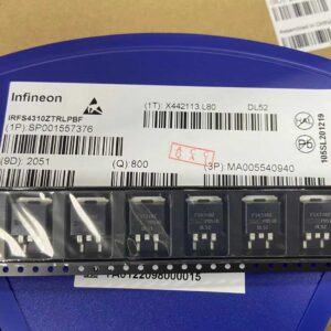
IRFS4310ZTRLPBF

IRFS4310ZTRLPBF – 100V N-Channel HEXFET Power MOSFET, 7 mΩ RDS(on), D2PAK (TO-263AB)

Brand: infineon

Package: D2PAK (TO-263AB)

IN STOCK: 11137pcs

Cargo cycle: 3-7 Days

The minimum order is 1

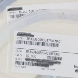
MSASJ105BB5475MFNA01

4.7uF 6.3V X5R MLCC, 0402, Taiyo Yuden

Brand: gigadevice

Package: 0402 (1005 Metric, 1.0 x 0.5 x 0.5 mm)

IN STOCK: 9701pcs

Cargo cycle: 3-7 Days

The minimum order is 1

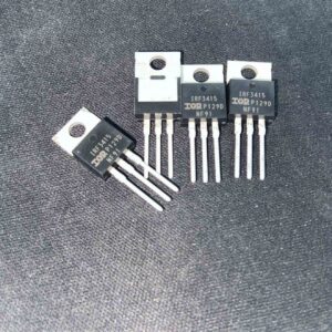
IRF3415PBF

150V N-channel power MOSFET, 43A, 41mΩ RDS(on), TO-220AB package

Brand: infineon

Package: TO-220AB

IN STOCK: 2940pcs

Cargo cycle: 3-7 Days

The minimum order is 1

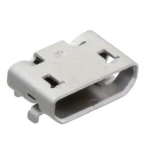
105017-1001

USB Type-C receptacle connector, 24-pin, SMD

Brand: Amphenol

Package: SMD (8.9 x 7.3 x 3.2 mm, right angle)

IN STOCK: 5335pcs

Cargo cycle: 3-7 Days

The minimum order is 1

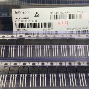
IRLB3034PBF

IRLB3034PBF – 40V N-Channel StrongIRFET Power MOSFET (Logic Level), 1.7 mΩ (max) @ 10V; 2.0 mΩ @ 4.5V RDS(on), TO-220AB

Brand: infineon

Package: TO-220AB

IN STOCK: 9724pcs

Cargo cycle: 3-7 Days

The minimum order is 1

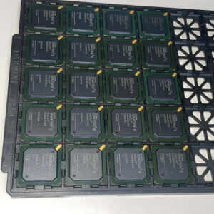
XC6SLX75-2FGG484I

Spartan-6 LX75 FPGA, 74637 logic cells, 132 DSP, 3096KB BRAM, 408 I/O, FBGA-484 23x23mm, -2 speed, industrial -40~100C, AMD Xilinx

Brand: xilinx

Package: FGG484 (484-ball fine-pitch BGA, 23x23mm body, 1.0mm ball pitch, 22×22 ball array, 6 I/O banks, lead-free)

IN STOCK: 890pcs

Cargo cycle: 3-7 Days

The minimum order is 1