Opens in a new tab

CD4012BE

Dual 4-input NAND gate, CMOS 3-18V, 60ns, PDIP-14

3000

Effective Inventory

Image for reference only

Manufacturer Part:

CD4012BE

Package:

PDIP-14 (19.3 x 6.35 x 4.57mm, 2.54mm pitch, through-hole)

Brand:

Quality Commitment

Shipping & Payment

Service & Packaging

Product Manual

Other recommendations you may be interested in.

Description

Product Overview

The CD4012BE from Texas Instruments contains two independent 4-input NAND gates — the CMOS counterpart of the SN74LS20N for 3V-18V systems in a 14-pin PDIP package.

Key Specifications

Number of Gates 2 (dual 4-input NAND)
Technology CD4000B CMOS
Supply Voltage 3V to 18V
Propagation Delay 60ns typical @ VDD=10V
Quiescent Current 0.01µA typical @ 25°C
Operating Temperature -55°C to +125°C
Package PDIP-14 (19.3 x 6.35mm)

Features

  • Dual 4-input NAND gates
  • Wide supply voltage: 3V to 18V
  • Output LOW only when all four inputs are HIGH
  • Near-zero quiescent current

Applications

  • Multi-condition decoding
  • Address decoding in CMOS systems
  • Control logic for battery-powered designs
  • General CMOS logic
Product Introduction: CD4012BE Product Introduction

The CD4012BE from Texas Instruments contains two independent 4-input NAND gates. Each gate implements Y = NOT(A AND B AND C AND D); the output goes LOW only when all four inputs are simultaneously HIGH. The CD4012 is the CMOS equivalent of the TTL 7420, with the advantage of 3V-18V supply range and near-zero quiescent current. The 4-input NAND is essential for address decoding and multi-condition logic in CMOS systems. For example, to generate an active-LOW chip select when a 4-bit address matches a specific pattern, the CD4012 directly provides the decoded output. The wide supply range allows the CD4012 to be used in 12V automotive systems, 9V battery circuits, and 3.3V/5V digital logic — all with the same IC. The BE suffix denotes the PDIP-14 package.

Working Principle: CD4012BE Working Principle

Each 4-input NAND gate in the CD4012BE performs Y = (A·B·C·D)’. The output is LOW only when all four inputs A, B, C, D are HIGH. For any other combination (at least one input LOW), the output is HIGH. The CMOS implementation uses a series PMOS network connecting the output to VDD (when any input is LOW, the PMOS network conducts, pulling output HIGH) and a series NMOS network connecting the output to VSS (when all inputs are HIGH, the NMOS network conducts, pulling output LOW). This series structure for 4 inputs is more complex than 2-input gates but provides the same basic NAND function with wider input capability. Unused inputs must be tied to VDD or VSS — never left floating (CMOS inputs are very high impedance and will drift to undefined levels). Tie unused inputs to VDD to make them logically ‘1’ (don’t care in NAND).

Pin Description: CD4012BE Pin Definition and Functions
Pin Name Type Description
1 1Y Output Gate 1 output
2 1A Input Gate 1 input A
3 1B Input Gate 1 input B
4 1C Input Gate 1 input C
5 1D Input Gate 1 input D
6 NC — No connection
7 VSS Power Ground
8 NC — No connection
9 2A Input Gate 2 input A
10 2B Input Gate 2 input B
11 2C Input Gate 2 input C
12 2D Input Gate 2 input D
13 2Y Output Gate 2 output
14 VDD Power Supply (3V to 18V)

CD4012BE uses the PDIP-14 package with standard CMOS 4000-series pinout convention: VDD at Pin 14, VSS at Pin 7. Each of the two NAND gates uses four input pins and one output pin — Gate 1 uses Pins 1-4 (inputs) and Pin 13 (output), Gate 2 uses Pins 9-12 (inputs) and Pin 6 (output). Pins 5 and 8 are not connected internally. All unused CMOS inputs MUST be tied to VDD or VSS to prevent floating-gate oscillation and excessive supply current. The CD4012BM is the SOIC-14 surface-mount equivalent with identical pinout. For TTL-compatible input levels, the 74HC20 (2.0-6.0V) or 74LS20 (4.75-5.25V) provides the same dual 4-input NAND function.

Application Scenarios: In which products and applications is CD4012BE used
  • 4-Bit Address Decode: 4 address lines (with inverters as needed) → 1A-1D; 1Y goes LOW only for target address; 1Y → active-LOW chip select
  • All-HIGH Detection: 4 status signals → A,B,C,D; Y = LOW when all 4 are HIGH; all-systems-go detector (inverted)
  • 12V Logic Decode: VDD=12V; 4 control signals at 12V levels; NAND output drives 12V logic directly; no level shifting needed
  • Battery-Powered Gating: VDD=9V battery; 4 sensor inputs; NAND output = alarm when all sensors active; near-zero standby current
Alternative Models: What chips are recommended as replacements for CD4012BE
Model Manufacturer Key Difference Package Supply
CD4012BM TI SOIC-14 surface-mount version with identical logic function and 3-18V range SOIC-14 3-18V
CD4012BE TI Through-hole DIP version for prototyping and legacy board repair DIP-14 3-18V
HEF4012BT NXP Pin-compatible CMOS version with improved ESD protection and 3-15V supply SOIC-14 3-15V
MC144012BDR2G onsemi Pin-compatible equivalent with RoHS compliance and AEC-Q100 automotive option SOIC-14 3-18V
74HC20D TI/Nexperia HC CMOS version with higher speed and 2-6V supply for modern logic systems SOIC-14 2-6V
74HC20N TI/Nexperia HC CMOS through-hole version for prototyping with 2-6V supply range DIP-14 2-6V
74HCT20D Nexperia HCT version with TTL-compatible inputs for mixed 5V TTL/CMOS systems SOIC-14 4.5-5.5V

CD4012 is the CMOS 4000-series dual 4-input nand gate operating over the wide 3-18V supply range. The HEF4012 (NXP) and MC144012 (onsemi) are direct pin-compatible equivalents. For higher speed at the cost of narrower voltage range, the 74HC20 HC/HCT families offer significantly faster propagation delay and lower power consumption at 2-6V. Surface-mount versions use the BM/M suffix (SOIC); through-hole versions use the BE suffix (DIP).

Recommend Parts

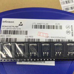
IRFS4310ZTRLPBF

IRFS4310ZTRLPBF – 100V N-Channel HEXFET Power MOSFET, 7 mΩ RDS(on), D2PAK (TO-263AB)

Brand: infineon

Package: D2PAK (TO-263AB)

IN STOCK: 11137pcs

Cargo cycle: 3-7 Days

The minimum order is 1

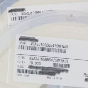
MSASJ105BB5475MFNA01

4.7uF 6.3V X5R MLCC, 0402, Taiyo Yuden

Brand: gigadevice

Package: 0402 (1005 Metric, 1.0 x 0.5 x 0.5 mm)

IN STOCK: 9701pcs

Cargo cycle: 3-7 Days

The minimum order is 1

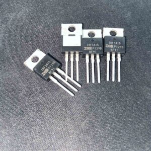
IRF3415PBF

150V N-channel power MOSFET, 43A, 41mΩ RDS(on), TO-220AB package

Brand: infineon

Package: TO-220AB

IN STOCK: 2940pcs

Cargo cycle: 3-7 Days

The minimum order is 1

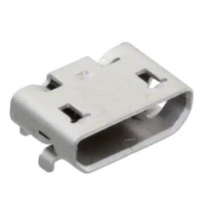
105017-1001

USB Type-C receptacle connector, 24-pin, SMD

Brand: Amphenol

Package: SMD (8.9 x 7.3 x 3.2 mm, right angle)

IN STOCK: 5335pcs

Cargo cycle: 3-7 Days

The minimum order is 1

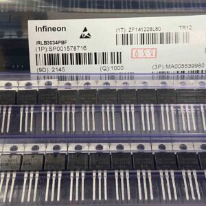
IRLB3034PBF

IRLB3034PBF – 40V N-Channel StrongIRFET Power MOSFET (Logic Level), 1.7 mΩ (max) @ 10V; 2.0 mΩ @ 4.5V RDS(on), TO-220AB

Brand: infineon

Package: TO-220AB

IN STOCK: 9724pcs

Cargo cycle: 3-7 Days

The minimum order is 1

XC6SLX75-2FGG484I

Spartan-6 LX75 FPGA, 74637 logic cells, 132 DSP, 3096KB BRAM, 408 I/O, FBGA-484 23x23mm, -2 speed, industrial -40~100C, AMD Xilinx

Brand: xilinx

Package: FGG484 (484-ball fine-pitch BGA, 23x23mm body, 1.0mm ball pitch, 22×22 ball array, 6 I/O banks, lead-free)

IN STOCK: 890pcs

Cargo cycle: 3-7 Days

The minimum order is 1