
Opens in a new tab

CD4018BE

5-stage Johnson counter, presettable divide-by-N (2-10), CMOS 3-18V, PDIP-16

2000

Effective Inventory

Image for reference only

Manufacturer Part:

CD4018BE

Package:

PDIP-16 (19.3 x 9.4 x 4.57mm, 2.54mm pitch, through-hole)

Brand:

Quality Commitment

Shipping & Payment

Service & Packaging

Product Manual

Other recommendations you may be interested in.

Description

Product Overview

The CD4018BE from Texas Instruments is a CMOS presettable divide-by-N counter using a 5-stage Johnson counter architecture — capable of dividing by any integer from 2 to 10 (or higher with cascading) in a 16-pin PDIP package.

Key Specifications

Function 5-stage Johnson counter, presettable divide-by-N
Technology CD4000B CMOS
Supply Voltage 3V to 18V
Counter Stages 5 (Johnson/Johnson counter)
Max Clock Frequency 10MHz typical @ VDD=10V
Trigger Positive edge on CLK
Reset Asynchronous, active HIGH (RST)
Preset 5 individual JAM inputs + PRESET ENABLE (active HIGH)
Outputs Q1, Q2, Q3, Q4, Q5 (buffered)
Data Input DATA (serial, for feedback configuration)
Operating Temperature -55°C to +125°C
Package PDIP-16 (19.3 x 9.4mm)

Features

  • Johnson counter architecture — spike-free decoded outputs
  • Divide by 2, 3, 4, 5, 6, 7, 8, 9, or 10 with simple feedback
  • 5 individual JAM inputs for presetting
  • Anti-lock gating ensures correct counting sequence
  • Schmitt trigger clock input
  • 3V-18V wide supply range

Applications

  • Programmable frequency dividers
  • Frequency synthesizers
  • Counter/timer control
  • Sequence generation
Product Introduction: CD4018BE Product Introduction

The CD4018BE from Texas Instruments is a 5-stage Johnson counter with preset capability, designed for programmable divide-by-N applications. Unlike binary ripple counters that divide only by powers of 2, the CD4018 can divide by any integer from 2 to 10 using simple feedback connections. The Johnson counter architecture produces spike-free outputs (unlike ripple counters) because only one bit changes per clock cycle. The divide ratio is set by feeding back one of the Q outputs (or its complement via a gate) to the DATA input: feed Q5̄ back for ÷10, Q4̄ for ÷8, Q3̄ for ÷6, Q2̄ for ÷4, Q1̄ for ÷2. For odd divisors (÷9, ÷7, ÷5, ÷3), a CD4011 gate combines two Q outputs before feeding back to DATA. The 5 JAM inputs (J1-J5) allow the counter to be preset to any Johnson state when PRESET ENABLE is HIGH, enabling programmable counters in frequency synthesizers. Multiple CD4018s can be cascaded for divisors greater than 10. The anti-lock gating ensures the counter always enters a valid Johnson sequence. The BE suffix denotes the PDIP-16 package.

Working Principle: CD4018BE Working Principle

The CD4018BE uses a 5-stage Johnson counter (also called twisted-ring counter). In a Johnson counter, the complement of the last stage is fed back to the first stage. Starting from all zeros: 00000→10000→11000→11100→11110→11111→01111→00111→00011→00001→00000. This 10-state cycle naturally divides by 10. The DATA input replaces the feedback when externally connected. For ÷10: Q5̄ → DATA (10 states). For ÷8: Q4̄ → DATA (8 states). For ÷6: Q3̄ → DATA. For ÷4: Q2̄ → DATA. For ÷2: Q1̄ → DATA. For odd divisors, a gate is needed: ÷9 uses Q5̄ AND Q1, ÷7 uses Q4̄ AND Q1, ÷5 uses Q3̄ AND Q1, ÷3 uses Q2̄ AND Q1. When PRESET ENABLE is HIGH, the JAM inputs (J1-J5) load directly into the counter stages on the next clock edge, overriding the DATA feedback. This allows starting the count at any state, enabling programmable division. The RESET input (RST=HIGH) clears all stages to 0. The anti-lock gating detects invalid states (Johnson counters can get stuck in unused states) and forces the counter into a valid sequence.

Pin Description: CD4018BE Pin Definition and Functions
Pin Name Type Description
1 J5 Input Jam input for stage 5 (preset)
2 Q1 Output Stage 1 output
3 Q2 Output Stage 2 output
4 Q3 Output Stage 3 output
5 Q4 Output Stage 4 output
6 Q5 Output Stage 5 output
7 RST Input Reset (active HIGH, clears all stages)
8 VSS Power Ground
9 CLK Input Clock (positive edge triggered)
10 PE Input Preset enable (active HIGH, loads J1-J5)
11 J1 Input Jam input for stage 1 (preset)
12 J2 Input Jam input for stage 2 (preset)
13 J3 Input Jam input for stage 3 (preset)
14 J4 Input Jam input for stage 4 (preset)
15 DATA Input Serial data input (feedback for divide ratio)
16 VDD Power Supply (3V to 18V)
Application Scenarios: In which products and applications is CD4018BE used
  • Divide-by-10: Q5 through inverter (or CD4069) → DATA; CLK input frequency; Q5 = CLK/10; no external gate needed if Q5̄ is available via inverter
  • Divide-by-7 (Odd): CD4011 NAND gate: Q4 AND Q1 → invert → DATA; produces 7-state cycle
  • Programmable Divider: Switch selects which Q output feeds back to DATA; 5-position switch = divide by 2,4,6,8,10
  • Frequency Synthesizer: Three CD4018s cascaded; each decade set via JAM inputs from thumbwheel switch; divide by 2-999
Alternative Models: What chips are recommended as replacements for CD4018BE
Model Manufacturer Key Difference Package Supply
CD4018BM TI SOIC-16 surface-mount version with identical logic function and 3-18V range SOIC-16 3-18V
CD4018BE TI Through-hole DIP version for prototyping and legacy board repair DIP-16 3-18V
HEF4018BT NXP Pin-compatible CMOS version with improved ESD protection and 3-15V supply SOIC-16 3-15V
MC144018BDR2G onsemi Pin-compatible equivalent with RoHS compliance and AEC-Q100 automotive option SOIC-16 3-18V
74HC190D TI/Nexperia HC CMOS version with higher speed and 2-6V supply for modern logic systems SOIC-16 2-6V
74HC190N TI/Nexperia HC CMOS through-hole version for prototyping with 2-6V supply range DIP-16 2-6V
74HCT190D Nexperia HCT version with TTL-compatible inputs for mixed 5V TTL/CMOS systems SOIC-16 4.5-5.5V

CD4018 is the CMOS 4000-series presettable divide-by-n counter operating over the wide 3-18V supply range. The HEF4018 (NXP) and MC144018 (onsemi) are direct pin-compatible equivalents. For higher speed at the cost of narrower voltage range, the 74HC190 HC/HCT families offer significantly faster propagation delay and lower power consumption at 2-6V. Surface-mount versions use the BM/M suffix (SOIC); through-hole versions use the BE suffix (DIP).

Recommend Parts

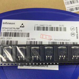
IRFS4310ZTRLPBF

IRFS4310ZTRLPBF – 100V N-Channel HEXFET Power MOSFET, 7 mΩ RDS(on), D2PAK (TO-263AB)

Brand: infineon

Package: D2PAK (TO-263AB)

IN STOCK: 11137pcs

Cargo cycle: 3-7 Days

The minimum order is 1

MSASJ105BB5475MFNA01

4.7uF 6.3V X5R MLCC, 0402, Taiyo Yuden

Brand: gigadevice

Package: 0402 (1005 Metric, 1.0 x 0.5 x 0.5 mm)

IN STOCK: 9701pcs

Cargo cycle: 3-7 Days

The minimum order is 1

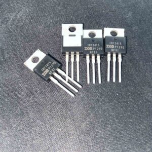
IRF3415PBF

150V N-channel power MOSFET, 43A, 41mΩ RDS(on), TO-220AB package

Brand: infineon

Package: TO-220AB

IN STOCK: 2940pcs

Cargo cycle: 3-7 Days

The minimum order is 1

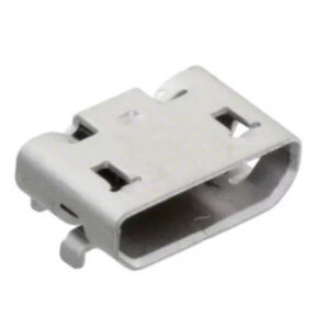
105017-1001

USB Type-C receptacle connector, 24-pin, SMD

Brand: Amphenol

Package: SMD (8.9 x 7.3 x 3.2 mm, right angle)

IN STOCK: 5335pcs

Cargo cycle: 3-7 Days

The minimum order is 1

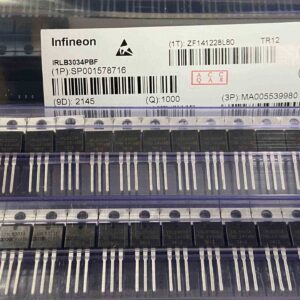
IRLB3034PBF

IRLB3034PBF – 40V N-Channel StrongIRFET Power MOSFET (Logic Level), 1.7 mΩ (max) @ 10V; 2.0 mΩ @ 4.5V RDS(on), TO-220AB

Brand: infineon

Package: TO-220AB

IN STOCK: 9724pcs

Cargo cycle: 3-7 Days

The minimum order is 1

XC6SLX75-2FGG484I

Spartan-6 LX75 FPGA, 74637 logic cells, 132 DSP, 3096KB BRAM, 408 I/O, FBGA-484 23x23mm, -2 speed, industrial -40~100C, AMD Xilinx

Brand: xilinx

Package: FGG484 (484-ball fine-pitch BGA, 23x23mm body, 1.0mm ball pitch, 22×22 ball array, 6 I/O banks, lead-free)

IN STOCK: 890pcs

Cargo cycle: 3-7 Days

The minimum order is 1