Opens in a new tab

Home » Integrated Circuits ICs, Interface ICs » CY7C1069G30-10ZSXI

CY7C1069G30-10ZSXI

16Mbit sync SRAM, 10ns, 100MHz, NoBL, VFBGA-54

2100

Effective Inventory

Image for reference only

Manufacturer Part:

CY7C1069G30-10ZSXI

Package:

54-Ball VFBGA (8.0 x 11.0 x 1.0 mm)

Brand:

Quality Commitment

Shipping & Payment

Service & Packaging

Product Manual

Description

Product Overview

The CY7C1069G30-10ZSXI is an Infineon (Cypress) 16Mbit (1M x 16) synchronous SRAM with 10ns access time, 3.3V supply, and NoBL (No Bus Latency) pipelined architecture. It supports 100MHz clock frequency for high-performance embedded processing. Packaged in 54-ball VFBGA, -40C to +85C.

Key Specifications

Capacity 16 Mbit (1M x 16)
Access Time 10 ns
Clock Freq 100 MHz
Supply 3.3 V
Architecture NoBL Pipelined
Package 54-ball VFBGA

Features

  • 16Mbit synchronous SRAM
  • 10ns access time, 100MHz clock
  • NoBL (No Bus Latency) pipelined
  • 3.3V single supply
  • 1M x 16-bit organization
  • Full synchronous operation
  • Byte-write capability

Applications

  • Networking and communications
  • Cache memory for processors
  • DSP and FPGA external RAM
  • High-speed data buffering
Product Introduction: CY7C1069G30-10ZSXI Product Introduction

The CY7C1069G30-10ZSXI is an Infineon (Cypress) 16Mbit (1M x 16) synchronous SRAM with NoBL (No Bus Latency) pipelined architecture and 10ns access time. The NoBL architecture eliminates the bus turnaround latency inherent in common I/O SRAMs when switching between read and write operations, providing back-to-back read/write capability without dead cycles. This is critical for networking applications where random read/write patterns dominate. The 100MHz clock frequency supports high-throughput packet processing and DSP algorithms. The 3.3V single supply is compatible with most FPGA and processor I/O standards. The 1M x 16-bit organization matches typical 16-bit processor data bus widths. The pipelined architecture registers the outputs, providing higher clock frequencies at the cost of one cycle of latency. Byte-write capability allows partial word updates. Packaged in 54-ball VFBGA rated for -40C to +85C.

Working Principle: CY7C1069G30-10ZSXI Working Principle

The CY7C1069G30 uses a pipelined synchronous SRAM architecture with the NoBL (No Bus Latency) feature. All inputs (address, data, control) are registered on the rising edge of the positive-edge-triggered clock (CLK). The pipelined architecture adds one cycle of latency from address presentation to data output, but allows higher clock rates than flow-through designs. The NoBL feature uses separate read and write data paths internally, allowing the device to perform a read immediately after a write (or vice versa) to the same address without inserting a dead bus turnaround cycle. This is implemented by maintaining separate read and write buffers and multiplexing them to the I/O pins based on the current operation. The synchronous interface provides address, data, and control inputs that are sampled on the clock edge, simplifying timing analysis in high-speed systems. The chip select (CE), output enable (OE), and byte-write enables (BWE) control the read/write operations.

Pin Description: CY7C1069G30-10ZSXI Pin Definition and Functions

54-ball VFBGA with key signals: A0-A19 (address), DQ0-DQ15 (data I/O), CLK (clock), CE (chip enable), OE (output enable), WE (write enable), BWE0/BWE1 (byte write enables), MODE (burst mode), ADSP/ADSC (address strobe), ADV (advance), ZZ (sleep). Refer to datasheet for complete 54-ball VFBGA ball map.

Application Scenarios: In which products and applications is CY7C1069G30-10ZSXI used
  • Networking switch/router packet buffer with NoBL for back-to-back read/write
  • Cache memory for embedded processors requiring 100MHz SRAM access
  • DSP and FPGA external RAM with 16-bit data width and 10ns latency
  • High-speed data buffering in communications and video processing
Alternative Models: What chips are recommended as replacements for CY7C1069G30-10ZSXI
Model Manufacturer Key Difference
CY7C1069G30-12ZSXI Infineon 12ns slower speed grade
CY7C1079G30 Infineon 8Mbit, smaller capacity
IS61NLF25636A ISSI Similar NoBL SRAM
IDT71T756 Renesas Similar sync SRAM

Recommend Parts

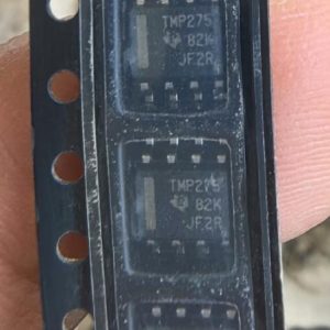
TMP275AIDR

0.5C I2C temp sensor, 12-bit, 2.7-5.5V, alert output, 8-SOIC

Brand: TI

Package: 8-SOIC (4.90 x 3.91 x 1.50 mm)

IN STOCK: 3681pcs

Cargo cycle: 3-7 Days

The minimum order is 1

IL485E

NVE IL485E IsoLoop isolated RS-485 transceiver, 2.5kVrms isolation, 35Mbps, 16-SOIC WB

Brand: nve

Package: SOIC-16 WB

IN STOCK: 5280pcs

Cargo cycle: 3-7 Days

The minimum order is 1

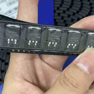
IRFS4227TRLPBF

IRFS4227TRLPBF – 200V N-Channel HEXFET PDP Switch Power MOSFET, 26 mΩ RDS(on), D2PAK (TO-263)

Brand: infineon

Package: D2PAK (TO-263)

IN STOCK: 4334pcs

Cargo cycle: 3-7 Days

The minimum order is 1

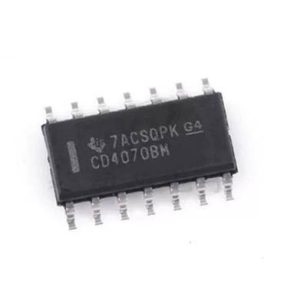
CD4070BM96

Quad 2-input XOR gate, 3-18V CMOS, 65ns at 10V, SOIC-14

Brand: TI

Package: SOIC-14 (8.75 x 3.9 x 1.5mm)

IN STOCK: 4245pcs

Cargo cycle: 3-7 Days

The minimum order is 1

AB1526

Bluetooth 5.0 Dual Mode Audio SoC, TWS, AAC, Dual-mic ENC, Integrated Charger, BGA

Brand: airoha

Package: BGA

IN STOCK: 25000pcs

Cargo cycle: 3-7 Days

The minimum order is 1

LP2980IM5-5.0

50mA micropower ultra-low-dropout regulator, 5V, SOT-23-5

Brand: TI

Package: SOT-23-5 (2.9 x 1.6 x 1.1 mm)

IN STOCK: 2557pcs

Cargo cycle: 3-7 Days

The minimum order is 1