

Opens in a new tab

Home » Integrated Circuits ICs » M29F040-90N1

M29F040-90N1

4Mbit 5V NOR Flash, 512KB x 8, 90ns access, 8 x 64KB sectors, 32-DIP, ST

12177

Effective Inventory

Image for reference only

Manufacturer Part:

M29F040-90N1

Package:

32-PDIP

Brand:

Product Categories:

Quality Commitment

Shipping & Payment

Service & Packaging

Product Manual

Other recommendations you may be interested in.

Description

Product Overview

The M29F040-90N1 is a 4Mbit (512KB x 8) 5V single-supply Flash memory from STMicroelectronics. This non-volatile memory device features 90ns access time and is organized as 524,288 words of 8 bits each. It offers uniform sector architecture with 8 sectors of 64KB each, supporting individual sector erase and full chip erase operations. The device can be programmed in-system using a standard 5V supply, and features advanced command set architecture compatible with the JEDEC standard for Flash memories. The 90N1 suffix indicates 90ns access time in a 32-pin plastic DIP package.

Key Specifications

Type 5V Flash Memory (NOR)
Memory Size 4 Mbit (512KB / 524,288 x 8 bits)
Access Time 90 ns (max)
Supply Voltage (VCC) 4.5V ~ 5.5V (5V nominal)
Sector Architecture 8 uniform sectors × 64KB each
Programming Method Byte program, 10µs/byte typical
Sector Erase Time 0.6s typical
Chip Erase Time 3s typical
Endurance 100,000 erase/program cycles
Data Retention 10 years minimum
Package 32-Pin Plastic DIP (PDIP)
Operating Temperature 0°C ~ +70°C (Commercial)

Features

  • 5V single supply for read, program, and erase
  • 4Mbit density (512KB x 8)
  • Fast access time: 90ns
  • Uniform 64KB sector architecture (8 sectors)
  • JEDEC standard command interface
  • Status register for operation monitoring
  • Byte program with embedded program algorithm
  • Sector erase and chip erase support
  • Hardware data protection scheme
  • Low power consumption
  • 100K program/erase cycles
  • 10-year data retention
  • RoHS compliant package

Applications

  • Embedded system firmware storage
  • Microcontroller program memory
  • Industrial control systems
  • Telecom equipment firmware
  • Automotive electronics
  • Set-top boxes and digital TV
  • Networking equipment
  • Medical devices
Product Introduction: M29F040-90N1 Product Introduction

The M29F040-90N1 is a 4 megabit (512KB) 5V single-supply NOR Flash memory from STMicroelectronics, organized as 524,288 bytes with 90ns maximum access time. Operating from a single 5V supply for both read and program/erase operations, it simplifies system design by eliminating the need for additional high-voltage supplies. The memory is organized into 8 uniform sectors of 64KB each, allowing flexible erase granularity — individual sectors can be erased without affecting other sectors, or the entire chip can be erased at once. The device uses an industry-standard command interface (JEDEC compatible) where read, program, and erase operations are initiated by writing specific command sequences to the device. An internal status register provides feedback on operation progress, including ready/busy status and error flags. The embedded algorithm automatically handles program and erase pulse timing, requiring only simple command sequences from the host controller. Hardware protection features include a write protect function and power-on write inhibit to prevent accidental programming during power transitions. The 32-pin plastic DIP package provides a rugged through-hole form factor compatible with standard PCB assembly. With 100,000 program/erase cycle endurance and 10-year data retention, the M29F040-90N1 is suitable for firmware storage in embedded systems, industrial controls, telecom equipment, automotive electronics, and networking applications requiring reliable non-volatile memory.

Working Principle: M29F040-90N1 Working Principle

The M29F040 is a NOR-type Flash memory that stores data using floating gate transistor technology and operates from a single 5V supply. NOR architecture allows random access to any memory location for read operations, with the access time determined by the address-to-output delay (90ns). Each memory cell consists of a floating gate transistor where the presence or absence of trapped electrons on the floating gate determines the stored data (0 or 1). In the erased state, cells store ‘1’ (conducting), and programming sets cells to ‘0’ (non-conducting) by injecting electrons onto the floating gate via channel hot electron injection. Erasing removes electrons from the floating gate via Fowler-Nordheim tunneling. The device operates in three main modes: (1) Read mode — the default state after power-on, where address lines select a memory location and the corresponding data byte appears on the output pins. (2) Program mode — entered by writing a command sequence (0xAA/0x55/0xA0) followed by the address and data to be programmed. The internal state machine then performs the programming operation automatically, typically completing within 10µs per byte. (3) Erase mode — can be sector erase or chip erase, initiated by a specific command sequence. Erase time is typically 0.6s per sector or 3s for the full chip. During program or erase operations, the Status Register can be read to monitor progress — bit 7 (Data Polling) toggles until the operation completes, and bit 6 (Toggle Bit) provides another method of monitoring. Error bits indicate if the operation failed (e.g., due to endurance exhaustion). The 5V-only operation is achieved through integrated charge pumps that generate the higher voltages needed for program and erase operations internally.

Pin Description: M29F040-90N1 Pin Definition and Functions
Pin Number Pin Name Type Description
1 A15 Input Address line 15
2-9 A12-A7 Input Address lines 12 through 7
10-17 DQ0-DQ7 I/O Data input/output lines 0 through 7
18 GND Power Ground (0V)
19 DQ7 I/O Data line 7 (alternate pin ordering)
20-22 CE#, A0, A1 Mixed Chip Enable, Address 0, Address 1
23-29 A2-A6, A16 Input Address lines 2-6, 16
30 OE# Input Output Enable (active low)
31 WE# Input Write Enable (active low)
32 VCC Power Power supply (4.5V-5.5V)
Note: Exact pinout follows standard 32-pin DIP Flash memory pinout.
Application Scenarios: In which products and applications is M29F040-90N1 used
  • Embedded microprocessor firmware storage
  • Industrial controller program memory
  • Telecom switching equipment
  • Automotive body controllers
  • Set-top box firmware
  • Network router/switch boot code
  • Medical equipment firmware
  • Instrumentation and test gear
Alternative Models: What chips are recommended as replacements for M29F040-90N1
Manufacturer Part Number Description
STMicroelectronics M29F040B-70N1 4Mbit 5V Flash, 70ns, 32-DIP
AMD/Spansion AM29F040B-70PD 4Mbit 5V Flash, 70ns, 32-DIP
Intel 28F004B 4Mbit 5V Flash, 90ns, 32-DIP
Atmel AT29C040A-90PC 4Mbit 5V Flash, 90ns, 32-DIP

Recommend Parts

RK73B2ATTD100J

10Ohm +/-5% 0.125W thick film resistor, 0805, +/-200 ppm/C, AEC-Q200

Brand: KOA Speer

Package: 0805 (2012 Metric) 2.0 x 1.25 x 0.55 mm

IN STOCK: 26435pcs

Cargo cycle: 3-7 Days

The minimum order is 1

TPS77001DBVR

50mA LDO, adjustable 1.2-5.5V out, 35mV dropout, 17µA IQ, SOT-23-5

Brand: TI

Package: SOT-23-5 (2.9 x 1.6 x 1.45 mm)

IN STOCK: 5000pcs

Cargo cycle: 3-7 Days

The minimum order is 1

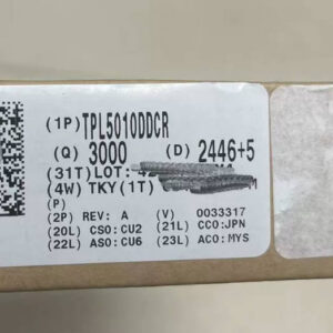
TPL5010DDCR

Nano-power watchdog timer with power good, SOT-23-6

Brand: TI

Package: SOT-23-6 (2.9 x 1.6 x 1.1 mm, DDC package)

IN STOCK: 12122pcs

Cargo cycle: 3-7 Days

The minimum order is 1

S1MB-13-F

1A 1000V GPP rectifier, 1.1V VF, 3μs trr, SMB/DO-214AA, -65~150°C

Brand: Diodes Inc

Package: SMB / DO-214AA (4.57 x 3.94 x 2.50mm)

IN STOCK: 3679pcs

Cargo cycle: 3-7 Days

The minimum order is 1

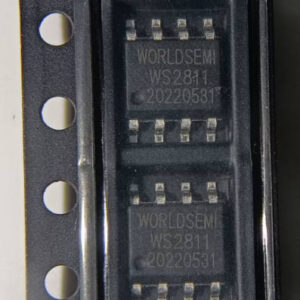
WS2811

3-channel LED driver IC with built-in oscillator, SOP-8

Brand: Worldsemi

Package: SOP-8 (5.2 x 4.0 mm)

IN STOCK: 7374pcs

Cargo cycle: 3-7 Days

The minimum order is 1

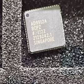
AD9912ABCPZ

1GSPS direct digital synthesizer with 14-bit DAC, LFCSP-64

Brand: ADI

Package: LFCSP-64 (9.0 x 9.0 mm, BCPZ package)

IN STOCK: 3719pcs

Cargo cycle: 3-7 Days

The minimum order is 1