Opens in a new tab

MAX660CSA+

Charge-pump voltage inverter/doubler, 1.5-5.5V in, 100mA out, SOIC-8

5455

Effective Inventory

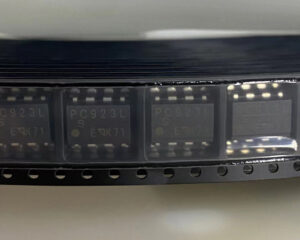
Image for reference only

Manufacturer Part:

MAX660CSA+

Package:

8-SOIC (4.9 x 3.9 x 1.75 mm, SA package)

Brand:

Quality Commitment

Shipping & Payment

Service & Packaging

Product Manual

Description

Product Overview

The MAX660CSA+ from Analog Devices (Maxim) is a monolithic CMOS charge-pump voltage converter that inverts or doubles an input voltage from 1.5V to 5.5V at up to 100mA output current in an 8-pin SOIC package.

Key Specifications

Function Charge-Pump Voltage Inverter / Doubler
Input Voltage 1.5V to 5.5V
Output Voltage -VIN (inverter) or 2x VIN (doubler)
Output Current 100 mA (max)
Conversion Efficiency 96% (typ, no load)
Output Resistance 6.5 Ohm (typ @ 5V, +25C)
Oscillator Frequency 10 kHz (internal) or up to 45kHz (external)
Supply Current 200 uA (typ @ 5V)
Package 8-SOIC (3.9mm width)
Operating Temperature 0 to +70 C

Features

  • Inverts or doubles input voltage
  • 100mA output current capability
  • 96% power conversion efficiency (no load)
  • Only 2 external capacitors required
  • Internal oscillator (10kHz) or external clock
  • Replace ICL7660 with improved performance
  • 6.5 Ohm output resistance (half of ICL7660)

Applications

  • Negative supply from positive rail (op-amp bias)
  • 5V to -5V conversion for RS-232
  • Battery voltage doubling
  • LCD contrast adjustment
Product Introduction: MAX660CSA+ Product Introduction

The MAX660CSA+ from Analog Devices (Maxim) is a monolithic CMOS charge-pump voltage converter that can invert a positive input voltage to its negative equivalent (e.g., +5V to -5V) or double the input voltage (e.g., +3V to +6V). The device requires only two external capacitors (typically 10uF to 150uF) for operation, making it one of the simplest voltage conversion solutions available. The MAX660 improves upon the classic ICL7660 with half the output resistance (6.5 Ohm typical vs. 12-15 Ohm for ICL7660 at 5V), delivering higher output current at lower voltage drop. The 100mA maximum output current and 96% no-load conversion efficiency make it suitable for moderate-power negative rail generation in op-amp circuits, RS-232 transceivers, and data acquisition systems. The internal oscillator operates at 10kHz, but the FC (frequency control) pin allows an external capacitor to increase the frequency up to 45kHz for lower output ripple, or an external clock can drive the OSC pin for precise frequency control. In inverter mode, the output voltage is approximately -VIN + (IOUT x ROUT), where ROUT is the output resistance. For example, with VIN=5V and IOUT=50mA, VOUT = -5V + (0.05A x 6.5Ohm) = -4.675V. In doubler mode, the output is approximately 2xVIN – (IOUT x ROUT). The MAX660CSA+ operates over the 0 to +70C temperature range and is available in an 8-pin SOIC package.

Working Principle: MAX660CSA+ Working Principle

The MAX660CSA+ operates using a flying-capacitor charge-pump (also called switched-capacitor) technique. Key subsystems include: (1) Charge Pump – the core of the device is a network of CMOS switches that alternately charge and discharge an external ‘flying’ capacitor (C1); during phase 1, C1 is connected between VIN and GND and charges to VIN; during phase 2, C1 is reconnected with its positive terminal to GND and negative terminal to the output; this effectively ‘pumps’ charge from VIN to VOUT, creating a negative output voltage; (2) Output Filter – a second external capacitor (C2) smooths the output voltage ripple; the ripple amplitude is approximately IOUT / (fOSC x C2); larger C2 or higher oscillator frequency reduces ripple; (3) Oscillator – the internal RC oscillator runs at approximately 10kHz; the FC pin selects between 10kHz (FC=V+ or open) and 45kHz (FC=GND) operation; alternatively, an external clock (up to 150kHz) can be applied to the OSC pin; higher frequencies reduce output ripple and allow smaller capacitors but increase supply current; (4) Doubler Mode – in voltage doubler configuration, the flying capacitor is charged to VIN during phase 1, and during phase 2 it is stacked on top of VIN (series-connected), producing approximately 2 x VIN at the output; the output capacitor C2 filters the result; (5) Efficiency – the conversion efficiency is determined by the ratio of output resistance to load resistance; at no load, efficiency is 96% (only quiescent current loss); at full load, efficiency decreases because more power is dissipated in the output resistance.

Pin Description: MAX660CSA+ Pin Definition and Functions
Pin Name Function
1 FC Frequency control (open/V+ = 10kHz, GND = 45kHz)
2 CAP+ Positive terminal of flying capacitor C1
3 GND Ground
4 CAP- Negative terminal of flying capacitor C1
5 VOUT Negative output voltage (inverter mode)
6 LV Low-voltage operation (GND for VIN > 3.5V, V+ for VIN < 3.5V)
7 OSC Oscillator input (external clock) or capacitor for freq adj
8 V+ Positive supply voltage (1.5V to 5.5V)
Application Scenarios: In which products and applications is MAX660CSA+ used
  • Op-amp dual supply: +5V to -5V at 50mA for dual-supply op-amp circuits with only 2 external capacitors
  • RS-232: +5V to -5V at 20mA for negative rail of 3.3V/5V RS-232 transceiver
  • Battery doubler: 3V lithium cell to 6V at 50mA for 5V logic systems
  • LCD contrast: +5V to -5V variable output for LCD VEE contrast adjustment
Alternative Models: What chips are recommended as replacements for MAX660CSA+
Manufacturer Part Number Package Notes
ADI/Maxim MAX660MJA CERDIP-8 Military temperature range
TI LMC7660IN DIP-8 ICL7660 compatible, higher Rout
ADI/Maxim MAX828EUK+T SOT-23-5 Smaller package, 25mA max
ADI/Maxim MAX680CPA DIP-8 Simultaneous +2xVIN and -VIN outputs

Recommend Parts

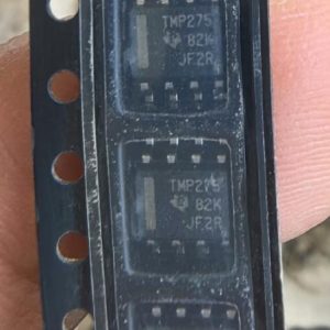
TMP275AIDR

0.5C I2C temp sensor, 12-bit, 2.7-5.5V, alert output, 8-SOIC

Brand: TI

Package: 8-SOIC (4.90 x 3.91 x 1.50 mm)

IN STOCK: 3681pcs

Cargo cycle: 3-7 Days

The minimum order is 1

IL485E

NVE IL485E IsoLoop isolated RS-485 transceiver, 2.5kVrms isolation, 35Mbps, 16-SOIC WB

Brand: nve

Package: SOIC-16 WB

IN STOCK: 5280pcs

Cargo cycle: 3-7 Days

The minimum order is 1

IRFS4227TRLPBF

IRFS4227TRLPBF – 200V N-Channel HEXFET PDP Switch Power MOSFET, 26 mΩ RDS(on), D2PAK (TO-263)

Brand: infineon

Package: D2PAK (TO-263)

IN STOCK: 4334pcs

Cargo cycle: 3-7 Days

The minimum order is 1

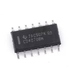
CD4070BM96

Quad 2-input XOR gate, 3-18V CMOS, 65ns at 10V, SOIC-14

Brand: TI

Package: SOIC-14 (8.75 x 3.9 x 1.5mm)

IN STOCK: 4245pcs

Cargo cycle: 3-7 Days

The minimum order is 1

AB1526

Bluetooth 5.0 Dual Mode Audio SoC, TWS, AAC, Dual-mic ENC, Integrated Charger, BGA

Brand: airoha

Package: BGA

IN STOCK: 25000pcs

Cargo cycle: 3-7 Days

The minimum order is 1

LP2980IM5-5.0

50mA micropower ultra-low-dropout regulator, 5V, SOT-23-5

Brand: TI

Package: SOT-23-5 (2.9 x 1.6 x 1.1 mm)

IN STOCK: 2557pcs

Cargo cycle: 3-7 Days

The minimum order is 1