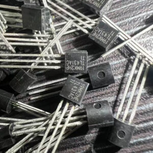

Product Overview
The MMBFJ113 from onsemi is an N-channel JFET switch with -0.5V to -3.0V cutoff voltage, 2mA IDSS, and SOT-23-3 package for low-level analog switching.
Key Specifications
| Type | N-Channel JFET Switch |
| VGS(off) (Cutoff Voltage) | -0.5V to -3.0V |
| IDSS (Zero-Gate Drain Current) | 2.0 mA (min) @ VDS=15V |
| rDS(on) | 100 Ohm (max) @ VDS=0.1V, VGS=0 |
| V(BR)GSS | -35 V (min) @ IG=-1uA |
| IGSS (Gate Leakage) | -1.0 nA (max) @ VGS=-15V |
| Power Dissipation | 350 mW @ TA=25C |
| RJA | 357 C/W |
| Package | SOT-23-3 (TO-236-3) |
| Operating Temperature | -55C to +150C (TJ) |
Features
- N-channel JFET for low-level analog switching
- 2mA IDSS minimum with -0.5V to -3.0V cutoff
- 100 Ohm max on-resistance
- Source and drain are interchangeable
Ultra-low gate leakage: -1.0 nA max - Designed for sample-and-hold and chopper circuits
Applications
- Sample-and-hold circuits
- Chopper-stabilized amplifiers
- Analog signal switching
- Low-level signal gating
Product Introduction: MMBFJ113 Product Introduction
The MMBFJ113 from onsemi is an N-channel junction field-effect transistor (JFET) designed for low-level analog switching applications in a SOT-23-3 surface-mount package. As a depletion-mode device, the JFET is normally-on (conducting) when VGS=0, with a minimum IDSS of 2.0mA at VDS=15V. The gate-source cutoff voltage (VGS(off)) ranges from -0.5V to -3.0V, meaning the channel is pinched off when VGS is negative enough to exceed the cutoff voltage. The 100 Ohm maximum on-resistance at VGS=0 provides low insertion loss for analog signals. The ultra-low gate leakage current (-1.0 nA maximum) ensures minimal offset current in sample-and-hold and chopper applications. Source and drain are interchangeable, simplifying PCB layout. The J113 is the lowest IDSS member of the J111/J112/J113 family (20mA/5mA/2mA respectively), optimized for the lowest on-resistance per unit of drain current.
Working Principle: MMBFJ113 Working Principle
The MMBFJ113 is an N-channel JFET where the gate forms a reverse-biased PN junction with the channel. At VGS=0, the channel is fully open and IDSS (drain current at zero gate voltage) flows, determined by the channel geometry and doping. As VGS becomes more negative, the depletion region around the gate extends further into the channel, narrowing the conductive path. When VGS reaches VGS(off) (-0.5V to -3.0V), the depletion region pinches off the channel entirely and drain current drops to essentially zero. In analog switch applications, the JFET is used in its low-resistance region (VGS=0 for ON, VGS less than VGS(off) for OFF). The gate leakage current is the reverse-biased PN junction leakage, typically sub-nanoampere, which is critical for sample-and-hold circuits where any gate current would cause charge to leak from the hold capacitor. The 100 Ohm on-resistance is determined by the channel length, width, and doping concentration. The interchangeability of source and drain is a feature of symmetric JFET geometry, unlike MOSFETs where the body diode creates asymmetry.
Pin Description: MMBFJ113 Pin Definition and Functions
Pin Name Type Function 1 Gate Input Gate terminal (reverse-biased PN junction) 2 Source Power Source terminal (interchangeable with Drain) 3 Drain Power Drain terminal (interchangeable with Source) Application Scenarios: In which products and applications is MMBFJ113 used
- Sample-and-hold circuit with MMBFJ113 as the sampling switch and 1nA max gate leakage for minimal droop on hold capacitor
- Chopper-stabilized amplifier input switch with 100 Ohm on-resistance and zero offset voltage
- Precision analog signal gating with depletion-mode normally-on operation for fail-safe designs
Alternative Models: What chips are recommended as replacements for MMBFJ113
Manufacturer Part Number Package Notes onsemi MMBFJ111 SOT-23-3 20mA IDSS, lower rDS(on) (30 Ohm) onsemi MMBFJ112 SOT-23-3 5mA IDSS, 50 Ohm rDS(on) onsemi J113 TO-92 Through-hole version NXP BF862 SOT-23-3 VHF/UHF amplifier JFET, higher IDSS InterFET 2N5457 TO-92 General purpose N-ch JFET Recommend Parts

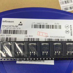
IRFS4310ZTRLPBF
IRFS4310ZTRLPBF – 100V N-Channel HEXFET Power MOSFET, 7 mΩ RDS(on), D2PAK (TO-263AB)
Brand: infineon
Package: D2PAK (TO-263AB)
IN STOCK: 11137pcs
Cargo cycle: 3-7 Days
The minimum order is 1
MSASJ105BB5475MFNA01
4.7uF 6.3V X5R MLCC, 0402, Taiyo Yuden
Brand: gigadevice
Package: 0402 (1005 Metric, 1.0 x 0.5 x 0.5 mm)
IN STOCK: 9701pcs
Cargo cycle: 3-7 Days
The minimum order is 1
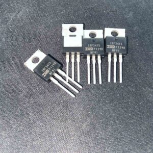
IRF3415PBF
150V N-channel power MOSFET, 43A, 41mΩ RDS(on), TO-220AB package
Brand: infineon
Package: TO-220AB
IN STOCK: 2940pcs
Cargo cycle: 3-7 Days
The minimum order is 1
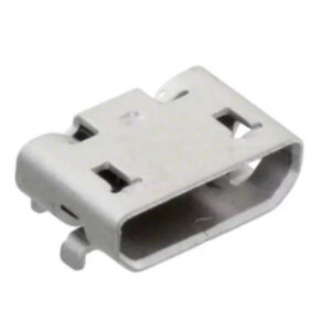
105017-1001
USB Type-C receptacle connector, 24-pin, SMD
Brand: Amphenol
Package: SMD (8.9 x 7.3 x 3.2 mm, right angle)
IN STOCK: 5335pcs
Cargo cycle: 3-7 Days
The minimum order is 1
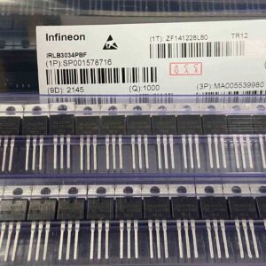
IRLB3034PBF
IRLB3034PBF – 40V N-Channel StrongIRFET Power MOSFET (Logic Level), 1.7 mΩ (max) @ 10V; 2.0 mΩ @ 4.5V RDS(on), TO-220AB
Brand: infineon
Package: TO-220AB
IN STOCK: 9724pcs
Cargo cycle: 3-7 Days
The minimum order is 1
XC6SLX75-2FGG484I
Spartan-6 LX75 FPGA, 74637 logic cells, 132 DSP, 3096KB BRAM, 408 I/O, FBGA-484 23x23mm, -2 speed, industrial -40~100C, AMD Xilinx
Brand: xilinx
Package: FGG484 (484-ball fine-pitch BGA, 23x23mm body, 1.0mm ball pitch, 22×22 ball array, 6 I/O banks, lead-free)
IN STOCK: 890pcs
Cargo cycle: 3-7 Days
The minimum order is 1