Opens in a new tab

Home » Integrated Circuits ICs » SN74HC259DR

SN74HC259DR

8-bit addressable latch, 4 functional modes, 2-6V, 14ns tpd, SOIC-16

2458

Effective Inventory

Image for reference only

Manufacturer Part:

SN74HC259DR

Package:

SOIC-16 (D) 9.9×3.9 mm

Brand:

Product Categories:

Quality Commitment

Shipping & Payment

Service & Packaging

Product Manual

Other recommendations you may be interested in.

Description

Product Overview

The SN74HC259DR from Texas Instruments is an 8-bit addressable latch in an SOIC-16 package, operating from 2V to 6V. It functions as an addressable latch, memory, 1-of-8 decoder/demultiplexer, or clear-mode device depending on CLR and enable (G) input states, providing versatile storage and decoding for digital systems.

Key Specifications

Logic Family HC (High-speed CMOS)
Channels 8-bit addressable
Supply Voltage 2V – 6V
Propagation Delay 14 ns (typical @ 5V)
Output Drive +/-5.2 mA @ 5V
Quiescent Current 80 uA max (8 uA typical)
Address Inputs 3 (S0, S1, S2)
Output Type Push-pull, non-inverting
Package SOIC-16 (9.9×3.9 mm)
Temperature -40 to +85 deg C

Features

  • Four distinct functional modes: addressable latch, memory, 1-of-8 decoder, and clear
  • Master reset (CLR) for asynchronous clearing of all outputs
  • Enable input (G) simplifies expansion for n-bit applications
  • Low 80 uA max quiescent current for power-efficient operation
  • High-current outputs can drive up to 10 LSTTL loads

Applications

  • Working registers and serial-holding registers in digital systems
  • 1-of-8 active-high decoding and demultiplexing
  • LED and display multiplexing drivers
  • General-purpose digital storage and address decoding
  • Peripheral I/O expansion for microcontrollers
Product Introduction: SN74HC259DR Product Introduction

The SN74HC259 is an 8-bit addressable latch from Texas Instruments designed for general-purpose storage applications in digital systems. It can operate in four distinct modes depending on the CLR and G (enable) input states: addressable latch mode (data written to addressed latch), memory mode (all latches hold previous state), 1-of-8 demultiplexer mode (addressed output follows data input), and clear mode (all outputs low). The 3-bit address selects one of 8 output latches. With low quiescent current and push-pull outputs capable of driving 10 LSTTL loads, it is a versatile building block for digital logic systems.

Working Principle: SN74HC259DR Working Principle

The SN74HC259 contains 8 transparent D-latches selected by a 3-to-8 decoder (S0, S1, S2). The D (data) input feeds all latches, but only the addressed latch is enabled to accept new data when G is LOW and CLR is HIGH. Unaddressed latches retain their previous state. When G goes HIGH (with CLR HIGH), all latches enter memory mode, ignoring data and address changes. When CLR is LOW and G is LOW, the device acts as a 1-of-8 demultiplexer where the addressed output follows D and all others are LOW. When CLR is LOW and G is HIGH, all outputs are forced LOW (clear mode) regardless of address and data.

Pin Description: SN74HC259DR Pin Definition and Functions
Pin Name Type Function
1 S0 Input Address bit 0
2 D Input Data input
3 Y7 Output Latch output 7
4 Y6 Output Latch output 6
5 Y5 Output Latch output 5
6 Y4 Output Latch output 4
7 Y3 Output Latch output 3
8 GND Power Ground
9 Y2 Output Latch output 2
10 Y1 Output Latch output 1
11 Y0 Output Latch output 0
12 CLR Input Master reset (active low)
13 G Input Enable (active low)
14 S2 Input Address bit 2
15 S1 Input Address bit 1
16 VCC Power Supply (2-6V)
Application Scenarios: In which products and applications is SN74HC259DR used
  • LED display multiplexing: 1-of-8 decoder drives individual digit selects
  • I/O expansion: microcontroller writes to 8 outputs via 3 address + 1 data line
  • Serial-to-parallel conversion: clock data into addressed latches sequentially
  • Address decoding: generate chip select signals from 3-bit address bus
  • Digital control systems: store control states in addressable latches
Alternative Models: What chips are recommended as replacements for SN74HC259DR
Manufacturer Part Number Package Notes
TI SN74HC259N PDIP-16 Same function, through-hole
TI SN74HC259PW TSSOP-16 Same function, TSSOP
Nexperia 74HC259D SOIC-16 Pin-compatible alternative
onsemi MC74HC259ADR2G SOIC-16 HC family equivalent
TI SN74LS259N PDIP-16 LS TTL variant

Recommend Parts

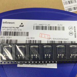
IRFS4310ZTRLPBF

IRFS4310ZTRLPBF – 100V N-Channel HEXFET Power MOSFET, 7 mΩ RDS(on), D2PAK (TO-263AB)

Brand: infineon

Package: D2PAK (TO-263AB)

IN STOCK: 11137pcs

Cargo cycle: 3-7 Days

The minimum order is 1

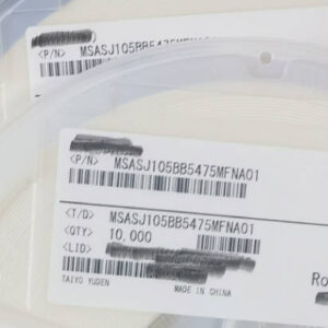
MSASJ105BB5475MFNA01

4.7uF 6.3V X5R MLCC, 0402, Taiyo Yuden

Brand: gigadevice

Package: 0402 (1005 Metric, 1.0 x 0.5 x 0.5 mm)

IN STOCK: 9701pcs

Cargo cycle: 3-7 Days

The minimum order is 1

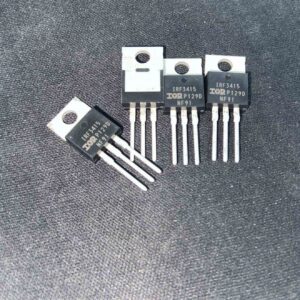
IRF3415PBF

150V N-channel power MOSFET, 43A, 41mΩ RDS(on), TO-220AB package

Brand: infineon

Package: TO-220AB

IN STOCK: 2940pcs

Cargo cycle: 3-7 Days

The minimum order is 1

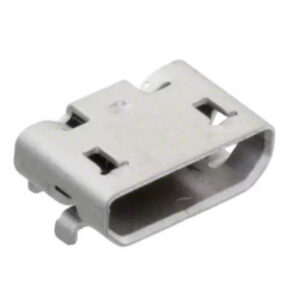
105017-1001

USB Type-C receptacle connector, 24-pin, SMD

Brand: Amphenol

Package: SMD (8.9 x 7.3 x 3.2 mm, right angle)

IN STOCK: 5335pcs

Cargo cycle: 3-7 Days

The minimum order is 1

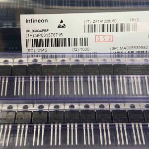
IRLB3034PBF

IRLB3034PBF – 40V N-Channel StrongIRFET Power MOSFET (Logic Level), 1.7 mΩ (max) @ 10V; 2.0 mΩ @ 4.5V RDS(on), TO-220AB

Brand: infineon

Package: TO-220AB

IN STOCK: 9724pcs

Cargo cycle: 3-7 Days

The minimum order is 1

XC6SLX75-2FGG484I

Spartan-6 LX75 FPGA, 74637 logic cells, 132 DSP, 3096KB BRAM, 408 I/O, FBGA-484 23x23mm, -2 speed, industrial -40~100C, AMD Xilinx

Brand: xilinx

Package: FGG484 (484-ball fine-pitch BGA, 23x23mm body, 1.0mm ball pitch, 22×22 ball array, 6 I/O banks, lead-free)

IN STOCK: 890pcs

Cargo cycle: 3-7 Days

The minimum order is 1