Opens in a new tab

SN74LS76AN

Dual J-K flip-flop, negative-edge, preset/clear, LS TTL, PDIP-16

4000

Effective Inventory

Image for reference only

Manufacturer Part:

SN74LS76AN

Package:

PDIP-16 (19.3 x 6.35 x 4.57mm, 2.54mm pitch, through-hole)

Brand:

Quality Commitment

Shipping & Payment

Service & Packaging

Product Manual

Other recommendations you may be interested in.

Description

Product Overview

The SN74LS76AN from Texas Instruments contains two independent J-K flip-flops with complementary outputs, preset and clear — more versatile than the D flip-flop 7474 thanks to J-K logic in a 16-pin PDIP package.

Key Specifications

Number of Flip-Flops 2 (dual, independent)
Logic Family LS (Low-power Schottky)
Trigger Type Negative-edge (falling edge of CLK)
Supply Voltage 4.75V to 5.25V
Max Clock Frequency 30MHz typical
J, K Inputs Level-triggered (set before clock edge)
Preset (PRE) Active-LOW (asynchronous, sets Q=1)
Clear (CLR) Active-LOW (asynchronous, sets Q=0)
Propagation Delay 15-20ns (CLK to Q)
Operating Temperature 0°C to +70°C
Package PDIP-16 (19.3 x 6.35mm)

Features

  • Dual J-K negative-edge-triggered flip-flops
  • J=0,K=0: hold; J=1,K=0: set; J=0,K=1: reset; J=1,K=1: toggle
  • Asynchronous preset and clear (active-LOW)
  • Complementary outputs (Q and NOT-Q)
  • 30MHz clock frequency

Applications

  • Toggle flip-flop / frequency divider
  • Data register
  • Counter building block
  • Control logic
Product Introduction: SN74LS76AN Product Introduction

The SN74LS76AN from Texas Instruments contains two independent J-K negative-edge-triggered flip-flops with direct preset (PRE, active-LOW) and clear (CLR, active-LOW). The J-K flip-flop is more versatile than the D flip-flop because it has four operating modes: hold (J=0,K=0), set (J=1,K=0), reset (J=0,K=1), and toggle (J=1,K=1). The toggle mode makes the 7476 ideal for frequency division: connecting J and K both HIGH causes Q to toggle on each falling clock edge, dividing the clock by 2. The 7476 triggers on the negative (falling) edge of the clock, unlike the 7474 which triggers on the positive (rising) edge. The asynchronous PRE and CLR override the clock: PRE=LOW forces Q=1; CLR=LOW forces Q=0. Both PRE and CLR must be HIGH for normal clocked operation. The 7476 is used in counter designs, control sequencers, and wherever J-K functionality is needed. The A suffix denotes the improved LS version; the N suffix denotes the PDIP-16 through-hole package.

Working Principle: SN74LS76AN Working Principle

Each J-K flip-flop in the SN74LS76AN captures the J and K input states on the falling edge of CLK and updates the Q output accordingly. Truth table (on falling CLK edge): J=0,K=0 → Q holds; J=1,K=0 → Q=1 (set); J=0,K=1 → Q=0 (reset); J=1,K=1 → Q toggles. The J and K inputs must be stable before the falling clock edge (setup time ~10ns). Asynchronous inputs override: PRE=LOW forces Q=1 regardless of CLK, J, K; CLR=LOW forces Q=0. Both PRE and CLR active simultaneously (both LOW) is invalid (Q and NOT-Q both HIGH). For toggle mode: J=K=1; each falling clock edge toggles Q; Q frequency = CLK/2. For frequency division by 4: cascade two 7476 flip-flops in toggle mode; Q1 → CLK2; Q2 frequency = CLK/4. For a 2-bit binary counter: two 7476s in toggle mode, Q1 drives CLK2; Q1,Q0 count 00→01→10→11→00. For a controlled set/reset: J and K control what happens on the next clock edge; J=1 sets, K=1 resets, both=1 toggles, both=0 holds.

Pin Description: SN74LS76AN Pin Definition and Functions
Pin Name Type Description
1 1CLR Input Flip-flop 1 clear (active LOW)
2 1Q Output Flip-flop 1 Q output
3 1NOT-Q Output Flip-flop 1 complementary output
4 1J Input Flip-flop 1 J input
5 VCC Power Supply (5V)
6 1CLK Input Flip-flop 1 clock (negative edge)
7 1K Input Flip-flop 1 K input
8 1PRE Input Flip-flop 1 preset (active LOW)
9 2PRE Input Flip-flop 2 preset (active LOW)
10 2K Input Flip-flop 2 K input
11 2CLK Input Flip-flop 2 clock (negative edge)
12 GND Power Ground
13 2J Input Flip-flop 2 J input
14 2NOT-Q Output Flip-flop 2 complementary output
15 2Q Output Flip-flop 2 Q output
16 2CLR Input Flip-flop 2 clear (active LOW)
Application Scenarios: In which products and applications is SN74LS76AN used
  • Toggle / ÷2: J=K=1 (tied HIGH); clock on CLK; Q toggles each falling edge; Q = CLK/2
  • 2-Bit Ripple Counter: FF1: J=K=1, clock=input; Q1→CLK2; FF2: J=K=1; Q2,Q1 = 2-bit count (00→01→10→11)
  • Controlled Latch: J=data, K=NOT-data; on falling CLK, Q captures data value (equivalent to D flip-flop with inverter)
  • Gated Oscillator: J=enable, K=enable; enable=1 → toggle; enable=0 → hold; gated clock output on Q
Alternative Models: What chips are recommended as replacements for SN74LS76AN
Model Manufacturer Key Difference Package Supply
74LS76N TI/Nexperia Original TTL version with 5V-only supply, typical propagation delay 10-15ns DIP-16 5V TTL
74LS76D TI/Nexperia Surface-mount SOIC version of LS with identical logic function SOIC-16 5V TTL
74HC76D TI/Nexperia CMOS version with wide 2-6V supply range, lower power consumption and higher noise immunity SOIC-16 2-6V CMOS
74HC76N TI/Nexperia Through-hole DIP version of HC family for prototyping and repair DIP-16 2-6V CMOS
74HCT76D TI/Nexperia CMOS with TTL-compatible input levels, ideal for mixing with LS devices at 5V SOIC-16 4.5-5.5V TTL-in
74HCT76N TI/Nexperia Through-hole DIP version of HCT family for prototyping and repair DIP-16 4.5-5.5V TTL-in

The 7476 is a Dual J-K Flip-Flop with Clear and Preset. Family variants span from the original LS TTL (5V only) to modern LVC/AUP (down to 0.8V). HC and HCT versions offer 2-6V CMOS operation with HCT providing TTL-compatible input thresholds for mixed 5V systems. CD4000-series equivalents offer the widest 3-18V supply range at the cost of lower switching speed. DIP packages (N suffix) are through-hole; SOIC (D suffix) and TSSOP are surface-mount.

Recommend Parts

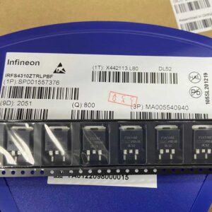
IRFS4310ZTRLPBF

IRFS4310ZTRLPBF – 100V N-Channel HEXFET Power MOSFET, 7 mΩ RDS(on), D2PAK (TO-263AB)

Brand: infineon

Package: D2PAK (TO-263AB)

IN STOCK: 11137pcs

Cargo cycle: 3-7 Days

The minimum order is 1

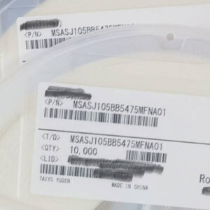
MSASJ105BB5475MFNA01

4.7uF 6.3V X5R MLCC, 0402, Taiyo Yuden

Brand: gigadevice

Package: 0402 (1005 Metric, 1.0 x 0.5 x 0.5 mm)

IN STOCK: 9701pcs

Cargo cycle: 3-7 Days

The minimum order is 1

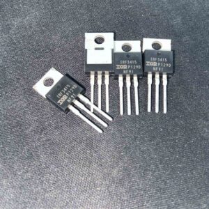
IRF3415PBF

150V N-channel power MOSFET, 43A, 41mΩ RDS(on), TO-220AB package

Brand: infineon

Package: TO-220AB

IN STOCK: 2940pcs

Cargo cycle: 3-7 Days

The minimum order is 1

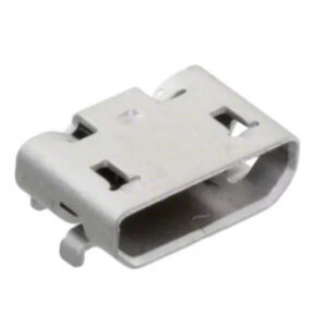
105017-1001

USB Type-C receptacle connector, 24-pin, SMD

Brand: Amphenol

Package: SMD (8.9 x 7.3 x 3.2 mm, right angle)

IN STOCK: 5335pcs

Cargo cycle: 3-7 Days

The minimum order is 1

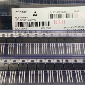
IRLB3034PBF

IRLB3034PBF – 40V N-Channel StrongIRFET Power MOSFET (Logic Level), 1.7 mΩ (max) @ 10V; 2.0 mΩ @ 4.5V RDS(on), TO-220AB

Brand: infineon

Package: TO-220AB

IN STOCK: 9724pcs

Cargo cycle: 3-7 Days

The minimum order is 1

XC6SLX75-2FGG484I

Spartan-6 LX75 FPGA, 74637 logic cells, 132 DSP, 3096KB BRAM, 408 I/O, FBGA-484 23x23mm, -2 speed, industrial -40~100C, AMD Xilinx

Brand: xilinx

Package: FGG484 (484-ball fine-pitch BGA, 23x23mm body, 1.0mm ball pitch, 22×22 ball array, 6 I/O banks, lead-free)

IN STOCK: 890pcs

Cargo cycle: 3-7 Days

The minimum order is 1