
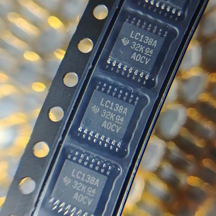

The SN74LVC138APWR from Texas Instruments is a 3-line to 8-line decoder/demultiplexer in a 16-pin TSSOP package, designed for high-performance memory decoding and data routing applications. The device features three binary-weighted address inputs (A0, A1, A2) that select one of eight active-low outputs (Y0-Y7). Three enable inputs (two active-low G2A, G2B and one active-high G1) provide flexible cascading for expansion to 24-line or 32-line decoders without external inverters. Operating voltage: 1.65V to 3.6V, with 5V-tolerant inputs for mixed-voltage systems. Maximum propagation delay: 5.8ns at 3.3V. Output drive: plus/minus 24mA. Quiescent current: 10uA max. Latch-up exceeds 250mA per JESD 17. -40C to 85C. MSL-1, RoHS, EAR99. Tape and reel, 2000/reel.
Home » Integrated Circuits ICs, Logic Chips » SN74LVC138APWR
SN74LVC138APWR
3-to-8 line decoder/demultiplexer, 1.65-3.6V, 5V-tolerant inputs, 5.8ns tpd, TSSOP-16, -40~85C
Effective Inventory
Manufacturer Part:
SN74LVC138APWR
Package:
TSSOP-16 (PW) (5.0 x 4.4 x 1.05 mm)
Brand:
Product Categories:
Quality Commitment
Shipping & Payment
Service & Packaging
Product Manual
Other recommendations you may be interested in.
Description
Product Introduction: SN74LVC138APWR Product Introduction
The SN74LVC138APWR from Texas Instruments is a 3-line to 8-line decoder/demultiplexer housed in a 16-pin TSSOP package, designed for high-performance memory decoding and data routing applications requiring very short propagation delay times.
The device features three binary-weighted address inputs (A0, A1, A2) that select one of eight mutually exclusive active-low outputs (Y0 through Y7). Three enable inputs provide flexible control: two active-low enables (G2A, G2B) and one active-high enable (G1). The decoder is enabled only when G1 is HIGH and both G2A and G2B are LOW. When disabled, all outputs are forced HIGH regardless of the address inputs.
The multiple enable inputs facilitate easy cascading for address expansion. Four SN74LVC138A devices plus one inverter can implement a 1-of-32 (5-to-32 line) decoder without additional logic. A single enable input can also serve as a data input for demultiplexing applications, distributing a single data stream to one of eight output lines.
Key specifications include: supply voltage 1.65V to 3.6V (single supply), 5.5V-tolerant inputs enabling use as a 3.3V-to-5V logic translator, maximum propagation delay of 5.8ns at 3.3V, output drive current of plus/minus 24mA, maximum quiescent current of 10uA, and latch-up performance exceeding 250mA per JESD 17. The typical output ground bounce is less than 0.8V and output VOH undershoot exceeds 2V at VCC=3.3V.
The LVC (Low-Voltage CMOS) technology provides the optimal combination of high speed, low power, and wide voltage compatibility. The 74LVC138A is functionally identical to the industry-standard 74LS138 and 74HC138 but with broader voltage range and 5V-tolerant inputs. The PW suffix denotes TSSOP-16 package, R suffix denotes tape and reel with 2,000 units per reel. The device is RoHS compliant, MSL Level 1, EAR99 classified.
Working Principle: SN74LVC138APWR Working Principle
The SN74LVC138APWR operates as a combinational logic decoder that converts a 3-bit binary address into one-of-eight active-low output selections, with enable inputs for cascading and demultiplexing.
Decoding Logic: The three address inputs A0 (LSB), A1, and A2 (MSB) form a 3-bit binary number from 0 to 7. Internally, the device implements eight 3-input AND gates, each fed by a unique combination of the address inputs (or their complements). For address value N, the corresponding output YN is driven LOW while all other outputs remain HIGH. Since all outputs are active-low, the selected output is the one that goes LOW. For example, if A2=0, A1=1, A0=0 (binary 010 = decimal 2), output Y2 goes LOW while Y0, Y1, Y3-Y7 remain HIGH.
Enable Logic: The three enable inputs (G1, G2A, G2B) gate all eight output AND gates. The decoder is enabled only when G1=HIGH AND G2A=LOW AND G2B=LOW. If any enable condition is not met, all eight outputs are forced HIGH regardless of the address inputs. The enable logic expression is: Enable = G1 AND (NOT G2A) AND (NOT G2B). The dual active-low enables (G2A, G2B) are particularly useful for cascading: one can serve as a chip select from higher-order address lines while the other provides system-level enable/disable control.
Cascading for Address Expansion: To build a 1-of-16 decoder, two SN74LVC138A devices are used. The most significant address bit (A3) connects to the enable inputs: one decoder is enabled when A3=0 (via G2A), and the other when A3=1 (via G1). For a 1-of-32 decoder, four devices are cascaded using a fifth address bit (A4) to select one of four decoder enable combinations. Two active-low enables and one active-high enable provide maximum flexibility in cascading configurations without requiring external inverters.
Demultiplexing Mode: When used as a demultiplexer, one of the enable inputs serves as the data input. For example, connecting the serial data stream to G1 while keeping G2A=G2B=LOW routes the data to the output selected by the current address. When the data input is HIGH, the selected output goes LOW (active); when LOW, all outputs go HIGH. This provides 1-to-8 data distribution under address control.
5V-Tolerant Inputs: The LVC family inputs can accept voltages up to 5.5V regardless of the VCC supply level. This enables the device to translate between 3.3V and 5V logic systems: a 5V microcontroller can drive the address and enable inputs of a 3.3V-supplied SN74LVC138A without level shifters. The output levels are determined by VCC, so the decoded outputs will be 3.3V logic levels.
Pin Description: SN74LVC138APWR Pin Definition and Functions
| Pin | Name | Type | Description |
|---|---|---|---|
| 1 | A0 | Input | Address input LSB; 5.5V tolerant; selects output line Y0-Y7 based on 3-bit binary value |
| 2 | A1 | Input | Address input middle bit; 5.5V tolerant; combines with A0 and A2 to select active output |
| 3 | A2 | Input | Address input MSB; 5.5V tolerant; determines which group of four outputs (Y0-3 or Y4-7) is active |
| 4 | /G2A | Input | Active-low enable input; decoder active only when G2A=LOW, G2B=LOW, and G1=HIGH simultaneously |
| 5 | /G2B | Input | Active-low enable input; can serve as chip select or data input for demultiplexing; 5.5V tolerant |
| 6 | G1 | Input | Active-high enable input; decoder enabled when HIGH with both G2A and G2B LOW; 5.5V tolerant |
| 7 | /Y7 | Output | Active-low decoded output 7; selected when A2A1A0 = 111; sinks up to 24mA |
| 8 | GND | Power | Ground; connect to system ground plane |
| 9 | /Y6 | Output | Active-low decoded output 6; selected when A2A1A0 = 110 |
| 10 | /Y5 | Output | Active-low decoded output 5; selected when A2A1A0 = 101 |
| 11 | /Y4 | Output | Active-low decoded output 4; selected when A2A1A0 = 100 |
| 12 | /Y3 | Output | Active-low decoded output 3; selected when A2A1A0 = 011 |
| 13 | /Y2 | Output | Active-low decoded output 2; selected when A2A1A0 = 010 |
| 14 | /Y1 | Output | Active-low decoded output 1; selected when A2A1A0 = 001 |
| 15 | /Y0 | Output | Active-low decoded output 0; selected when A2A1A0 = 000 |
| 16 | VCC | Power | Supply voltage; 1.65V to 3.6V; bypass with 0.1uF ceramic capacitor to GND |
Application Scenarios: In which products and applications is SN74LVC138APWR used
| Application | Description |
|---|---|
| Memory Address Decoding | Decodes upper address bits to generate chip select signals for multiple memory devices; 5.8ns propagation delay ensures zero wait-state operation with fast memories |
| I/O Port Expansion | Expands 3 microcontroller GPIO lines into 8 active-low chip select or enable lines; enables individual access to multiple peripheral ICs from limited MCU pins |
| Data Demultiplexing | Distributes a single data stream to one of eight output lines under address control; useful for time-division multiplexed signal routing |
| Address Expansion Cascading | Multiple SN74LVC138A devices cascade to build 1-of-16, 1-of-24, or 1-of-32 decoders; dual active-low and single active-high enables eliminate external logic |
| Mixed-Voltage Logic Translation | 5V-tolerant inputs allow 5V logic to drive 3.3V-supplied decoder; translates 5V address bus to 3.3V output levels without level shifters |
Alternative Models: What chips are recommended as replacements for SN74LVC138APWR
| Model | Manufacturer | Compatibility | Key Difference |
|---|---|---|---|
| 74HC138PW | Nexperia | Pin-Compatible | HC family (2-6V supply); same logic function; no 5V-tolerant input feature needed since supply can be 5V; different speed/voltage tradeoff |
| 74HCT138PW | Nexperia | Pin-Compatible | HCT family; 4.5-5.5V supply; TTL-compatible input thresholds; ideal for 5V systems interfacing with TTL logic |
| SN74LVC1G138 | TI | Functionally Equivalent | Single-gate version in tiny SOT-23-6 or VSSOP-8; same 3-to-8 decode; for space-constrained designs with fewer enable options |
| 74AHC138 | Renesas | Pin-Compatible | AHC family; 2-5.5V supply; faster than HC at 3.3V; intermediate between HC and LVC performance |
| SN74LVC139APWR | TI | Functionally Similar | Dual 2-to-4 decoder in same TSSOP-16; two independent decoders instead of one 3-to-8; different application scope |
Recommend Parts
RK73B2ATTD100J
10Ohm +/-5% 0.125W thick film resistor, 0805, +/-200 ppm/C, AEC-Q200
Brand: KOA Speer
Package: 0805 (2012 Metric) 2.0 x 1.25 x 0.55 mm
IN STOCK: 26435pcs
Cargo cycle: 3-7 Days
The minimum order is 1

TPS77001DBVR
50mA LDO, adjustable 1.2-5.5V out, 35mV dropout, 17µA IQ, SOT-23-5
Brand: TI
Package: SOT-23-5 (2.9 x 1.6 x 1.45 mm)
IN STOCK: 5000pcs
Cargo cycle: 3-7 Days
The minimum order is 1
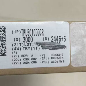
TPL5010DDCR
Nano-power watchdog timer with power good, SOT-23-6
Brand: TI
Package: SOT-23-6 (2.9 x 1.6 x 1.1 mm, DDC package)
IN STOCK: 12122pcs
Cargo cycle: 3-7 Days
The minimum order is 1
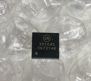
NCP302045MNTWG
45V 5A programmable overcurrent protection switch, 50mΩ Ron, -60V reverse polarity, DFN-8
Brand: ON
Package: DFN-8 (3x3mm, 0.65mm pitch)
IN STOCK: 4759pcs
Cargo cycle: 3-7 Days
The minimum order is 1
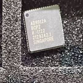
AD9912ABCPZ
1GSPS direct digital synthesizer with 14-bit DAC, LFCSP-64
Brand: ADI
Package: LFCSP-64 (9.0 x 9.0 mm, BCPZ package)
IN STOCK: 3719pcs
Cargo cycle: 3-7 Days
The minimum order is 1