Opens in a new tab

TPS5420DDAR

2A buck, 5.5-36V in, 500kHz, internal FET, SOIC-8

7119

Effective Inventory

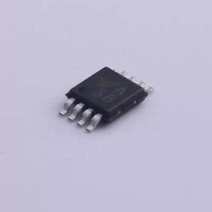
Image for reference only

Manufacturer Part:

TPS5420DDAR

Package:

SOIC-8 (4.9 x 6.0 x 1.58 mm)

Brand:

Quality Commitment

Shipping & Payment

Service & Packaging

Product Manual

Description

Product Overview

The TPS5420DDAR from Texas Instruments is a 2A, 500kHz step-down converter with 5.5-36V input range in an 8-pin SOIC package. With integrated 110mOhm N-channel MOSFET, internal compensation, adjustable output down to 1.22V, and up to 95% efficiency, it provides a simple and compact buck regulator solution.

Key Specifications

Topology Step-down (Buck) converter
Input Voltage Range 5.5V to 36V
Output Current 2A continuous, 3A peak
Output Voltage Adjustable 1.22V to 31V
Switching Frequency 500 kHz (fixed)
Integrated MOSFET Rds(on) 110 mOhm
Efficiency Up to 95%
Reference Voltage 1.22V, +/-1.5% initial accuracy
Quiescent Current 3 mA typical (operating)
Shutdown Current 18 uA typical (ENA low)
Control Mode Voltage mode with input feed-forward
Internal Compensation Yes (minimizes external components)
Max Duty Cycle 87%
Slow Start Internal (limits inrush current)
Protection OCP, OVP, thermal shutdown, UVLO
Operating Temperature -40 to +125 C (junction)
Package SOIC-8 (4.9 x 6.0 mm)
Status Active

Features

  • 5.5-36V wide input voltage range
  • 2A continuous output current
  • 110mOhm integrated MOSFET for high efficiency
  • Internal compensation reduces external component count
  • 500kHz fixed frequency for small filter components
  • Input voltage feed-forward improves line transient response
  • Internal slow start limits inrush current
  • Active-high enable with 18uA shutdown current
  • OCP, OVP, and thermal shutdown protection

Applications

  • 12V/24V distributed power systems
  • Industrial and automotive power supplies
  • Battery-powered equipment
  • Set-top boxes and networking equipment
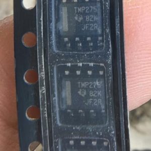
Product Introduction: TPS5420DDAR Product Introduction

The TPS5420DDAR from Texas Instruments is a 2A step-down (buck) switching regulator with integrated 110mOhm N-channel MOSFET in an 8-pin SOIC package. The DDA denotes the SOIC-8 (thermally enhanced) package, R denotes tape and reel (2500 pcs/reel). The device accepts a wide 5.5-36V input and produces an adjustable output from 1.22V to 31V at up to 2A continuous (3A peak). The 500kHz fixed switching frequency keeps the external inductor and capacitor values small, reducing solution size. The integrated 110mOhm high-side MOSFET eliminates the need for an external switch, reducing component count and ensuring high efficiency up to 95%. Internal compensation simplifies design by removing the need for external compensation components, though this limits the range of LC output filter values that can be used. Input voltage feed-forward maintains constant loop gain over the input range, improving line regulation and transient response compared to conventional voltage-mode control. An internal slow-start circuit limits inrush current during startup. The active-high ENA pin reduces quiescent current to 18uA in shutdown. Protection features include pulse-by-pulse overcurrent limiting, output overvoltage protection, undervoltage lockout (UVLO at 5.5V), and thermal shutdown.

Working Principle: TPS5420DDAR Working Principle

The TPS5420DDAR operates through five subsystems: (1) Power Stage: The integrated N-channel MOSFET connects VIN to the output through an external inductor. When the MOSFET is ON, current flows from VIN through the MOSFET and inductor to the output capacitor and load, storing energy in the inductor. When the MOSFET turns OFF, the external Schottky catch diode provides a path for inductor current to continue flowing to the output. (2) Voltage Mode Control with Feed-Forward: An internal error amplifier compares the FB pin voltage (from an external resistor divider on VOUT) with the 1.22V reference. The error amplifier output controls the PWM duty cycle. An input voltage feed-forward circuit adjusts the PWM ramp amplitude proportionally to VIN, maintaining constant loop gain and improving line transient response without requiring a change in compensation. (3) Internal Compensation: The error amplifier includes internal Type-II compensation (a zero and a pole), which is optimized for a specific range of output LC filter values. This simplifies design but requires the designer to choose inductor and capacitor values that work with the internal compensation. (4) Slow Start: An internal ramp gradually increases the duty cycle from zero to the regulation point over approximately 2ms, limiting inrush current in the output capacitor and preventing output overshoot. (5) Protection: Cycle-by-cycle current limiting (by monitoring the MOSFET current), output overvoltage protection (by comparing FB with an OVP threshold), UVLO (prevents operation below 5.5V), and thermal shutdown (disables output above approximately 165C junction temperature).

Pin Description: TPS5420DDAR Pin Definition and Functions
Pin Name Type Description
1 BOOT Power Bootstrap capacitor (connect to PH pin)
2 VIN Power Input voltage (5.5-36V)
3 PH Output Phase node (inductor connection)
4 GND Power Ground
5 VSENSE Input Feedback (connect to output divider)
6 ENA Input Enable (high=on, low=shutdown)
7 COMP I/O Error amplifier output / compensation
8 SS/SDA I/O Soft-start / sync (internal slow start)
Application Scenarios: In which products and applications is TPS5420DDAR used
  • 12V to 3.3V/2A point-of-load supply with 10uH inductor, 100uF output capacitor, 1N5822 Schottky diode, and 500kHz switching for compact solution size
  • 24V industrial bus to 5V/2A with 95% peak efficiency using internal MOSFET, internal compensation, and feed-forward for excellent line regulation
  • Battery-powered 4-cell Li-ion (10-16.8V) to 5V/1.5A with 18uA shutdown current and ENA pin for power gating
  • Set-top box 12V to 1.8V/2A core supply with internal slow start preventing output overshoot and OVP protecting downstream ICs
Alternative Models: What chips are recommended as replacements for TPS5420DDAR
Model Manufacturer Iout Vin Notes
TPS5430DDAR TI 3A 5.5-36V Higher current version
LM2596S-ADJ TI 3A 4.5-40V Lower freq (150kHz)
TPS54202DDCR TI 2A 4.5-28V Smaller package (SOT-23)
XL1509-5.0E1 XLSEMI 2A 4.5-40V Lower cost alternative

Recommend Parts

TMP275AIDR

0.5C I2C temp sensor, 12-bit, 2.7-5.5V, alert output, 8-SOIC

Brand: TI

Package: 8-SOIC (4.90 x 3.91 x 1.50 mm)

IN STOCK: 3681pcs

Cargo cycle: 3-7 Days

The minimum order is 1

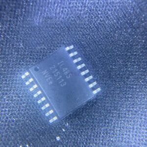
IL485E

NVE IL485E IsoLoop isolated RS-485 transceiver, 2.5kVrms isolation, 35Mbps, 16-SOIC WB

Brand: nve

Package: SOIC-16 WB

IN STOCK: 5280pcs

Cargo cycle: 3-7 Days

The minimum order is 1

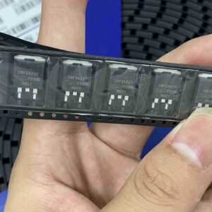
IRFS4227TRLPBF

IRFS4227TRLPBF – 200V N-Channel HEXFET PDP Switch Power MOSFET, 26 mΩ RDS(on), D2PAK (TO-263)

Brand: infineon

Package: D2PAK (TO-263)

IN STOCK: 4334pcs

Cargo cycle: 3-7 Days

The minimum order is 1

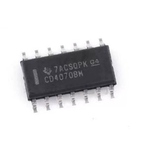
CD4070BM96

Quad 2-input XOR gate, 3-18V CMOS, 65ns at 10V, SOIC-14

Brand: TI

Package: SOIC-14 (8.75 x 3.9 x 1.5mm)

IN STOCK: 4245pcs

Cargo cycle: 3-7 Days

The minimum order is 1

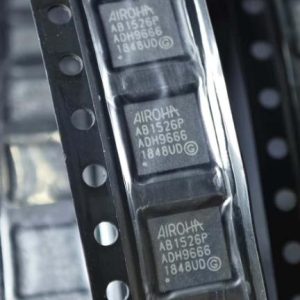
AB1526

Bluetooth 5.0 Dual Mode Audio SoC, TWS, AAC, Dual-mic ENC, Integrated Charger, BGA

Brand: airoha

Package: BGA

IN STOCK: 25000pcs

Cargo cycle: 3-7 Days

The minimum order is 1

LP2980IM5-5.0

50mA micropower ultra-low-dropout regulator, 5V, SOT-23-5

Brand: TI

Package: SOT-23-5 (2.9 x 1.6 x 1.1 mm)

IN STOCK: 2557pcs

Cargo cycle: 3-7 Days

The minimum order is 1