
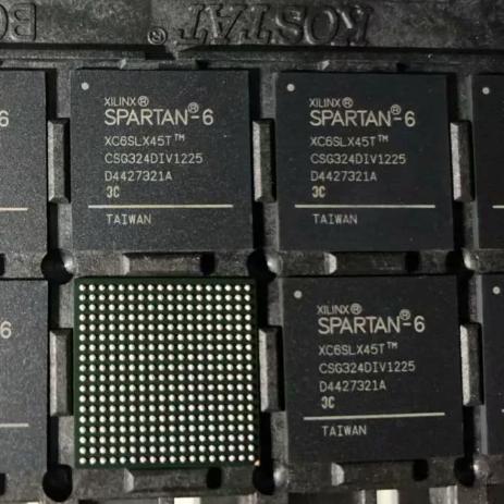
The XC6SLX45-3CSG324I from AMD/Xilinx is a Spartan-6 LX FPGA in a 324-pin CSBGA (chip-scale BGA) package with -3 speed grade (highest performance) and industrial temperature range. It features 43,661 logic cells, 2,088 Kbit block RAM, 58 DSP48A1 slices, 218 user I/Os, 4 CMTs (2 DCMs + 2 PLLs), and 1.2 V core voltage. Built on 45 nm low-power copper process. Supports DDR3 at 800 Mb/s, multiple I/O standards including LVDS, and MicroBlaze soft processor. Operating temperature range is -40C to +100C.
Home » Integrated Circuits ICs, Programmable Logic ICs (FPGA / CPLD) » XC6SLX45-3CSG324I
XC6SLX45-3CSG324I
Spartan-6 LX FPGA, 43661 LC, 2088Kb BRAM, 58 DSP, 218 I/O, CSG324, -3 speed, industrial
158
Effective Inventory
Manufacturer Part:
XC6SLX45-3CSG324I
Package:
CSBGA-324 (15x15mm, 0.8mm pitch, 1.0mm ball diameter)
Brand:
Product Categories:
Quality Commitment
Shipping & Payment
Service & Packaging
Product Manual
Other recommendations you may be interested in.
Description
Product Introduction: XC6SLX45-3CSG324I Product Introduction
The XC6SLX45-3CSG324I from AMD/Xilinx is a mid-range member of the Spartan-6 LX FPGA family in a 324-pin chip-scale BGA package with the highest -3 speed grade and industrial temperature range (-40C to +100C). The Spartan-6 family is built on a 45 nm low-power copper process technology that delivers approximately half the power consumption of the previous Spartan-3 generation.
The XC6SLX45 provides 43,661 logic cells organized into 6,822 adaptive logic modules (ALMs). Each ALM contains a 6-input look-up table (LUT) with dual flip-flops, enabling efficient implementation of both combinational and pipelined logic. The 3411 logic array blocks (LABs) provide the structural organization.
Memory resources include 2,088 Kbit of dual-port block RAM (116 x 18 Kb blocks, each optionally usable as two independent 9 Kb blocks) and 401 Kbit of distributed RAM for shift registers and small FIFOs. The block RAM supports byte-wide write enable and optional output pipeline registers for higher clock rates.
The 58 DSP48A1 slices provide dedicated hardware for high-performance arithmetic: 18 x 18 bit multipliers with 48-bit accumulators, pre-adders for filter applications, and cascading capability for wider operations. These DSP slices are ideal for FIR filters, FFTs, and motor control algorithms.
Four Clock Management Tiles (CMTs) each contain one Digital Clock Manager (DCM) and one Phase-Locked Loop (PLL). DCMs eliminate clock skew and duty-cycle distortion; PLLs provide low-jitter clock synthesis with fractional multiplication and division. Sixteen low-skew global clock networks distribute clocks throughout the device.
The CSG324 package provides 218 user I/Os supporting multiple standards including LVCMOS, LVTTL, SSTL, HSTL, and LVDS at up to 1,080 Mb/s per differential pair. The 0.8 mm pitch BGA is suitable for cost-sensitive, high-density PCB designs.
Configuration supports multiple modes including JTAG, Master/Slave Serial, and Master/Slave Parallel. The device supports MultiBoot for remote firmware upgrades with watchdog protection, and AES bitstream encryption for design security. The MicroBlaze soft processor enables embedded processing applications.
The XC6SLX45 is designed using the Xilinx ISE Design Suite. Note that the Spartan-6 family is a mature product; for new designs, AMD/Xilinx recommends the Spartan-7 or Artix-7 families with Vivado design tools.
Working Principle: XC6SLX45-3CSG324I Working Principle
**6-Input LUT Architecture:** Each logic cell contains a 6-input look-up table (LUT6) that can implement any 6-input Boolean function, or two 5-input functions with common inputs. The LUT output feeds two flip-flops that can be independently configured for edge-sensitive or level-sensitive operation. This dual-register architecture is optimized for pipeline-heavy DSP designs.
**Block RAM:** Each 18 Kb block RAM is a true dual-port memory with independent clocks, enables, and write enables for each port. Port widths are configurable from 1 to 36 bits. The optional output pipeline register adds one cycle of latency but enables higher clock frequencies.
**DSP48A1 Slice:** The DSP slice implements A x B + C where A and B are 18-bit inputs to the multiplier, and C is a 48-bit cascaded accumulator input. A pre-adder on the B input supports (A x (D+B)) + C for efficient filter tap implementation. The 48-bit output can cascade to adjacent DSP slices for wider operations.
**Clock Management Tile:** Each CMT contains one DCM and one PLL. The DCM provides delay-locked loop (DLL) functions: clock deskew, phase shifting (in 256 steps), and frequency synthesis (multiply/divide). The PLL provides similar functions with lower jitter and fractional frequency synthesis. The CMT can combine both for complex clock generation.
**Configuration and Security:** The FPGA loads its configuration from external flash memory (SPI, BPI, or JTAG) at power-up. AES-256 bitstream encryption protects the design from reverse engineering. The unique Device DNA identifier enables authentication. MultiBoot allows switching between multiple bitstreams for field upgrades.
Pin Description: XC6SLX45-3CSG324I Pin Definition and Functions
| Pin Group | Name | Type | Description |
|---|---|---|---|
| Multiple | VCCINT | P | Core supply voltage; 1.14-1.26V (nominal 1.2V); -3 speed grade; decouple with 0.1uF and 10uF capacitors near each VCCINT pin; high transient current demand during switching |
| Multiple | VCCO | P | I/O bank supply voltage; 1.14-3.6V depending on I/O standard; 6 independent I/O banks; each bank can use different VCCO for mixed-voltage interfacing; 3.3V for LVCMOS33, 2.5V for SSTL25, 1.8V for HSTL18 |
| Multiple | VCCAUX | P | Auxiliary supply; 2.5V nominal; powers PLLs, DCMs, and configuration logic; must be clean and stable; decouple carefully |
| 218 | I/O | I/O | User I/O pins; configurable as LVCMOS/LVTTL/SSTL/HSTL/LVDS; programmable slew rate and drive strength (up to 24mA); 5V tolerant with external resistor; bank-organized |
| Dedicated | JTAG | I/O | TCK, TMS, TDI, TDO; JTAG boundary scan and configuration access; 3.3V compatible; connect to JTAG header for programming and debug |
| Dedicated | CCLK/DIN | I/O | Configuration clock and data input; used in Master/Slave Serial configuration modes; CCLK output in Master mode, input in Slave mode |
| Dedicated | PROG_B | I | Program/erase control; active-low; pulling LOW initiates full device reconfiguration; connect to system reset or MCU GPIO for remote reconfiguration |
| Dedicated | INIT_B | O | Initialization status; LOW during configuration; HIGH when ready; open-drain; can signal configuration error; connect pull-up |
| Dedicated | DONE | O | Configuration done indicator; LOW during configuration; HIGH when device is configured and operational; open-drain with optional internal pull-up |
Application Scenarios: In which products and applications is XC6SLX45-3CSG324I used
| Application | Description |
|---|---|
| Industrial Vision Processing | Real-time image processing with camera interface (8-14 bit parallel up to 54 MB/s); DSP48A1 for pixel pipeline; block RAM for line buffers and frame storage; LVDS I/O for high-speed camera link; MicroBlaze for system control |
| Motor Control / Power Electronics | Multi-axis motor control with PWM generation; DSP48A1 for Park/Clarke transforms and PID; CMT for precise PWM carrier frequency; 218 I/O for multiple encoder and gate-driver interfaces; industrial temp range |
| Communication Bridge | Protocol bridging between legacy and modern interfaces; flexible I/O supports UART/SPI/I2C/parallel; block RAM for FIFO buffers; CSG324 package minimizes board area for space-constrained enclosures |
Alternative Models: What chips are recommended as replacements for XC6SLX45-3CSG324I
| Model | Manufacturer | Compatibility | Key Difference |
|---|---|---|---|
| XC6SLX45-2CSG324I | AMD/Xilinx | Lower Speed Grade | Same device in -2 speed grade; lower cost; lower performance; same package and pinout; drop-in replacement when timing margin allows |
| XC7A50T-1CSG325I | AMD/Xilinx | Next-Gen Upgrade | Artix-7; 52160 LC; 240 DSP; 16 GTP transceivers; 325-CSBGA; Vivado design tools; recommended for new designs; not pin-compatible |
| XC6SLX25-3CSG324I | AMD/Xilinx | Lower Density | 24051 LC; 936Kb BRAM; 38 DSP; same CSG324 package; drop-in compatible if design fits in smaller device; lower cost |
Recommend Parts
RK73B2ATTD100J
10Ohm +/-5% 0.125W thick film resistor, 0805, +/-200 ppm/C, AEC-Q200
Brand: KOA Speer
Package: 0805 (2012 Metric) 2.0 x 1.25 x 0.55 mm
IN STOCK: 26435pcs
Cargo cycle: 3-7 Days
The minimum order is 1

TPS77001DBVR
50mA LDO, adjustable 1.2-5.5V out, 35mV dropout, 17µA IQ, SOT-23-5
Brand: TI
Package: SOT-23-5 (2.9 x 1.6 x 1.45 mm)
IN STOCK: 5000pcs
Cargo cycle: 3-7 Days
The minimum order is 1
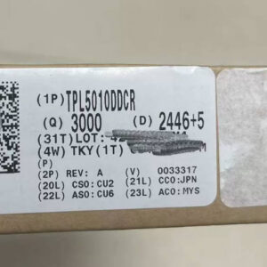
TPL5010DDCR
Nano-power watchdog timer with power good, SOT-23-6
Brand: TI
Package: SOT-23-6 (2.9 x 1.6 x 1.1 mm, DDC package)
IN STOCK: 12122pcs
Cargo cycle: 3-7 Days
The minimum order is 1
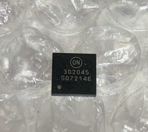
NCP302045MNTWG
45V 5A programmable overcurrent protection switch, 50mΩ Ron, -60V reverse polarity, DFN-8
Brand: ON
Package: DFN-8 (3x3mm, 0.65mm pitch)
IN STOCK: 4759pcs
Cargo cycle: 3-7 Days
The minimum order is 1
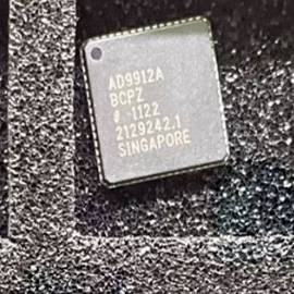
AD9912ABCPZ
1GSPS direct digital synthesizer with 14-bit DAC, LFCSP-64
Brand: ADI
Package: LFCSP-64 (9.0 x 9.0 mm, BCPZ package)
IN STOCK: 3719pcs
Cargo cycle: 3-7 Days
The minimum order is 1