






Opens in a new tab

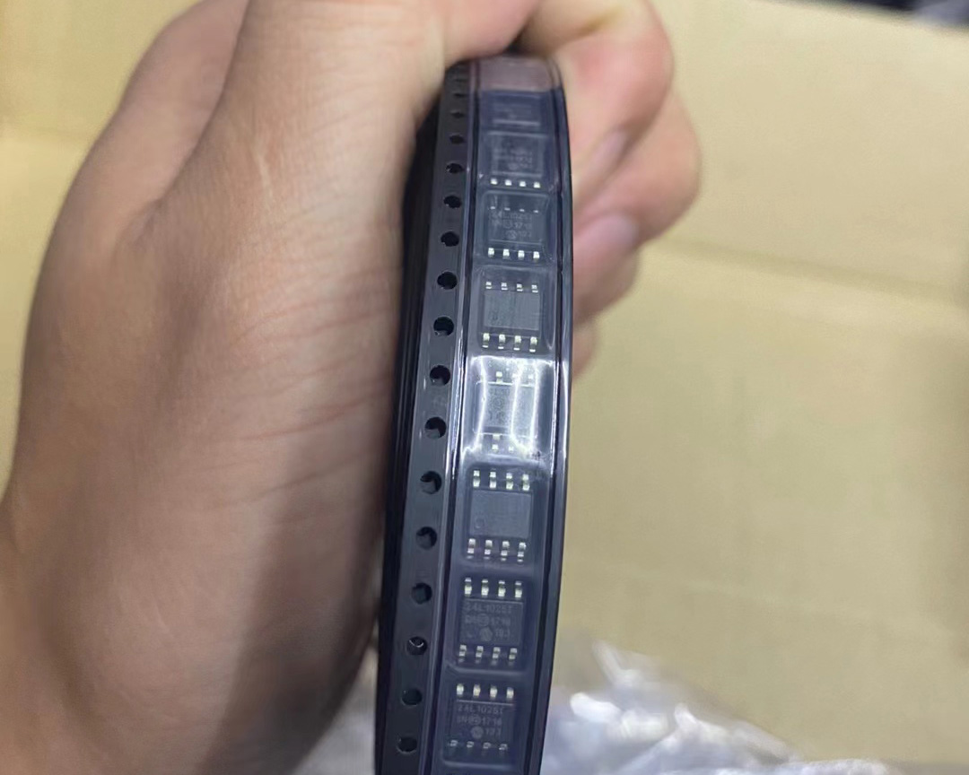
24LC1025-I

Microchip 24-series I2C EEPROM, 1Mbit, 128KB, 400kHz, 2.5-5.5V, 128B page, 1M cycles, 200yr retention, industrial -40~85°C, 8-pin

9500

Effective Inventory

Image for reference only

Manufacturer Part:

24LC1025-I

Package:

8-pin PDIP/SOIJ/SOIC/TSSOP/DFN options (suffix specifies package: P=PDIP, SM=SOIJ, SN=SOIC, ST=TSSOP, MC=DFN)

Brand:

Quality Commitment

Shipping & Payment

Service & Packaging

Product Manual

Description

Product Overview

The 24LC1025-I is a 1 Mbit (128 K x 8) I²C serial EEPROM from Microchip Technology, operating at 2.5 V to 5.5 V supply voltage with industrial temperature range (-40 °C to +85 °C). Part of Microchip’s widely used 24-series I²C EEPROM family, this device offers high density non-volatile memory with a simple 2-wire interface.

Organized as 131,072 bytes (128 KB), the 24LC1025 features both byte write and page write capability with a 128-byte page write buffer, enabling up to 128 bytes to be written in a single 5 ms write cycle. The device supports standard I²C bus speeds up to 400 kHz (Fast Mode). Schmitt trigger inputs on both SCL and SDA provide noise suppression, while output slope control minimizes ground bounce and EMI.

The 24LC1025 uses two address pins (A0, A1) with A2 internally biased, allowing up to four devices to be cascaded on the same I²C bus for a total of up to 4 Mbits of system EEPROM. A hardware Write-Protect (WP) pin enables protection of the entire memory array when pulled high. The device features over 1 million erase/write cycles and greater than 200-year data retention, making it suitable for long-lifecycle industrial and automotive applications.

Key Specifications

Parameter Value
Memory Type Serial EEPROM (non-volatile)
Memory Density 1 Mbit (1,024 Kbit)
Organization 128,000 x 8 bits (128 KB)
Interface I²C / 2-wire serial
Max Clock Frequency 400 kHz (Fast Mode)
Operating Voltage 2.5 V to 5.5 V
Page Size 128 bytes
Page Write Time 5 ms max (typical 3 ms)
Byte Write Time 5 ms max
Read Current (max) 450 µA @ 5.5 V
Standby Current (max) 5 µA @ 5.5 V
Write Protect Hardware WP pin (full array protection)
Address Pins A0, A1 (A2 internally tied to Vcc)
Max Cascaded Devices 4 devices per bus (up to 4 Mbit total)
Endurance 1,000,000 erase/write cycles
Data Retention > 200 years
ESD Protection > 4,000 V
Input Type Schmitt trigger (noise suppression)
Operating Temperature -40 °C to +85 °C (industrial, I grade)
Packages Available 8-pin PDIP, SOIJ/SOIC, TSSOP, DFN

Features

  • 1 Mbit (128 K x 8) I²C serial EEPROM
  • 2-wire I²C compatible interface
  • 400 kHz Fast Mode clock speed
  • 2.5 V to 5.5 V operating voltage range
  • 128-byte page write buffer
  • 5 ms max page write time
  • Hardware Write-Protect (WP) pin
  • Cascadable up to 4 devices on same bus
  • Schmitt trigger inputs for noise suppression
  • Output slope control to eliminate ground bounce
  • Sequential read capability
  • Random and sequential read modes
  • Self-timed write cycle with auto-erase
  • 450 µA max read current (very low power)
  • 5 µA max standby current
  • > 1,000,000 erase/write cycles endurance
  • > 200-year data retention
  • > 4 kV ESD protection on all pins
  • Factory programming available
  • Industrial temperature range: -40 to +85 °C
  • RoHS compliant, Pb-free
  • Automotive grade (AEC-Q100) versions available

Applications

  • Industrial control and factory automation
  • Automotive electronics and sensors
  • Consumer electronics and smart home
  • Data storage and configuration memory
  • IoT and wireless sensor nodes
  • Medical devices and equipment
  • Networking and telecom equipment
  • Power supply and battery management

Product Introduction: 24LC1025-I Product Introduction

The 24LC1025-I is a 1 Mbit (128 K x 8-bit) I2C serial EEPROM from Microchip Technology, offering high-density non-volatile memory with an industry-standard 2-wire interface. The -I suffix denotes industrial temperature range (-40°C to +85°C), and the LC designation indicates 2.5 V minimum operating voltage.

Organized as 131,072 bytes (128 KB), the 24LC1025 provides a large non-volatile storage solution for parameter storage, configuration data, calibration tables, event logs, and firmware backup. The device features both byte write and page write operations. The 128-byte page write buffer allows writing up to 128 contiguous bytes in a single write cycle (5 ms max), dramatically improving write throughput compared to byte-by-byte programming.

The I2C interface supports Standard Mode (100 kHz) and Fast Mode (400 kHz) operation, ensuring compatibility with virtually all microcontroller I2C peripherals. Schmitt trigger inputs on SCL and SDA provide excellent noise immunity in electrically noisy industrial environments. Output slope control helps minimize electromagnetic interference (EMI) and ground bounce.

Device addressing is provided by two external address pins (A0, A1), with A2 internally tied to Vcc. This allows cascading up to four 24LC1025 devices on the same I2C bus, for a total of up to 4 Mbits of system EEPROM memory. The internal A2-to-Vcc connection means the device always responds to addresses where the A2 bit is 1.

A hardware Write-Protect (WP) pin provides full-array write protection when pulled high, preventing accidental writes to the entire memory array. This is especially useful for protecting factory calibration data and other critical parameters from corruption due to software bugs or electrical transients.

The device features exceptional reliability with more than 1 million erase/write cycles per byte and greater than 200-year data retention. The self-timed write cycle includes automatic erase-before-program operation, requiring no external erase command. Factory pre-programming is available for high-volume applications.

Working Principle: 24LC1025-I Working Principle

The 24LC1025 is a serial EEPROM that stores data in floating-gate transistor cells and communicates via the I2C protocol. Here is how it works:

1. EEPROM Memory Array: The 1 Mbit memory array is organized as 128,000 x 8 bits. Data is stored in floating-gate MOSFET cells where the gate is electrically isolated by an oxide layer. Programming injects electrons onto the floating gate (changing the threshold voltage to represent a ‘0’), and erasing removes electrons (restoring the ‘1’ state). The data is non-volatile – it is retained for over 200 years without power.

2. I2C Interface: Communication is via a standard 2-wire I2C bus:
– SCL (Serial Clock): Clock signal generated by the master (MCU)
– SDA (Serial Data Address): Bidirectional data line
Both lines require pull-up resistors (typically 4.7 kΩ to Vcc). The 24LC1025 operates as a slave device. It supports I2C Standard Mode (100 kHz) and Fast Mode (400 kHz). Schmitt triggers on both inputs reject noise and slow-rising edges.

3. Device Addressing: The 7-bit device address is:
– 4 MSBs: ‘1010’ (fixed for 24-series EEPROMs)
– Next 2 bits: A1, A0 (set by external address pins)
– Bit 2 (A2): internally tied to Vcc (always 1)
– LSB: R/W bit (1 = read, 0 = write)
With 2 address pins, up to 4 devices can share the same bus.

4. Write Operation:
– Byte Write: Master sends device address (write), 17-bit memory address (2 byte address phase, using the A16 bit as part of the device address byte), then 1 data byte. EEPROM writes the byte into the addressed location. Self-timed write cycle takes up to 5 ms.
– Page Write: Similar to byte write, but master can send up to 128 data bytes after the address. All bytes are loaded into the 128-byte page write buffer, then programmed simultaneously into the selected page. Writes within a page boundary maximize efficiency.
– Acknowledge Polling: After initiating a write, the master can poll the device by sending its address. No ACK means write is still in progress; ACK means write is complete.

5. Read Operation:
– Current Address Read: Reads from the address last accessed + 1. No address phase needed.
– Random Read: Master sends device address (write) + memory address (sets address pointer), then repeated start + device address (read). EEPROM outputs the data byte.
– Sequential Read: After any read operation, if master ACKs the data byte, the address pointer auto-increments and the next byte is output. Can read entire memory array in one operation.

6. Write Protection: When WP pin is high, the entire memory array is write-protected. Attempted write operations are ignored. WP low allows normal write operation. Provides hardware protection against accidental writes.

7. Power Management:
– Active (Read): 450 µA max at 5.5V, 400 kHz
– Standby: 5 µA max at 5.5V
– Low-voltage detection: internal power-on reset ensures proper startup and prevents writes at low supply voltage

Pin Description: 24LC1025-I Pin Definition and Functions
Pin # Pin Name Type Description
1 A0 Input Address Input 0. Sets one bit of the I2C device address. Connect to Vss or Vcc (or leave floating – has internal pull-down). Must be hard-wired for proper operation. Allows up to 4 devices on same bus.
2 A1 Input Address Input 1. Sets second bit of I2C device address. Connect to Vss or Vcc. A2 is internally tied to Vcc (no pin available), limiting to 4 device addresses per bus.
3 WP Input Write Protect. When high (Vcc), entire memory array is write-protected. When low (Vss), normal read/write operation. Has internal pull-down resistor (can be left unconnected for normal operation). Used to protect factory calibration data and critical parameters.
4 Vss / GND Ground Ground / negative supply. Connect to system ground.
5 SDA I/O Serial Data Address. Bidirectional I2C data line. Open-drain output (requires external pull-up resistor, typically 4.7 kΩ to Vcc). Schmitt trigger input for noise immunity. Slope-controlled output for EMI reduction.
6 SCL Input Serial Clock. I2C clock input. Generated by bus master. Schmitt trigger input with noise suppression. Data is clocked in on SCL rising edge, out on falling edge.
7 Vss / GND Ground Ground / negative supply. Additional ground pin (Pin 7 is also Vss on some package variants, or may be N/C on others – check datasheet for specific package).
8 Vcc Power Positive power supply: 2.5 V to 5.5 V. Bypass with 0.1 µF ceramic capacitor to Vss. Decoupling capacitor should be placed as close to pin as possible.

8-Pin Pinout (PDIP, SOIC, TSSOP – top view):

    A0  1-+---+-8  Vcc
    A1  2-|   |-7  Vss (or N/C)
    WP  3-|   |-6  SCL
   GND  4-+---+-5  SDA

Note: Available in multiple package options. -I/P = 8-pin PDIP (through-hole), -I/SM = 8-pin SOIJ, -I/SN = 8-pin SOIC, -I/ST = 8-pin TSSOP, -I/MC = 8-pin DFN (surface mount). All have the same pinout. Industrial temperature range: -40°C to +85°C ambient. RoHS compliant, lead-free.

Application Scenarios: In which products and applications is 24LC1025-I used
  • Industrial Control and Factory Automation: PLC modules, industrial sensors, and fieldbus devices where large non-volatile storage is needed for configuration parameters, calibration data, device IDs, network settings, and event logs. The industrial temperature range and high reliability (200-year retention) meet the requirements of long-lifecycle industrial equipment.
  • Automotive Electronics and Sensors: Automotive ECUs, sensor modules, and body electronics requiring storage of calibration data, vehicle configuration, and fault codes. Automotive-grade versions (AEC-Q100 qualified) are available. The I2C interface allows simple connection to the microcontroller, and the 1 Mbit capacity stores comprehensive error logs and tuning parameters.
  • Consumer Electronics and Smart Home: Smart TVs, set-top boxes, home automation hubs, and IoT devices storing user preferences, Wi-Fi credentials, firmware parameters, and manufacturing data. The low standby current (5 µA) minimizes battery drain in always-on standby modes, and page writes enable fast bulk parameter updates.
  • Data Storage and Configuration Memory: Motherboards, network cards, graphics cards, and other computer peripherals storing BIOS/UEFI configuration, MAC addresses, serial numbers, and board-level parameters. Hardware write protection (WP pin) prevents accidental corruption of critical factory-programmed data.
  • IoT and Wireless Sensor Nodes: Battery-powered IoT devices and wireless sensor nodes storing sensor calibration coefficients, network parameters, and data logs for batch upload. The low active current (450 µA read) and 5 µA standby current minimize power consumption, extending battery life in energy-harvesting and battery-powered applications.
  • Medical Devices and Equipment: Patient monitors, diagnostic equipment, and medical sensors storing device calibration, patient data logs, and configuration parameters. The high endurance (1M cycles) supports frequent data logging, and the non-volatile nature ensures data survives power loss in clinical environments.
  • Networking and Telecom Equipment: Routers, switches, gateways, and optical transceivers storing configuration data, port parameters, firmware images, and statistical counters. Up to 4 devices can be cascaded on a single I2C bus for increased memory capacity, enabling modular designs with multiple EEPROMs per board.
  • Power Supply and Battery Management: Battery chargers, power supply modules, and BMS (Battery Management Systems) storing battery parameters, charge cycles, manufacturing data, and calibration values. The 2.5 V to 5.5 V wide operating range works with various system supply voltages, and the I2C interface allows the MCU to read/write parameters during operation.
Alternative Models: What chips are recommended as replacements for 24LC1025-I
Manufacturer Part Number Density Interface Voltage Page Size Notes
Microchip 24AA1025-I/SM 1 Mbit I2C 1.8-5.5 V 128 B Lower voltage (AA version)
Microchip 24FC1025-I/SN 1 Mbit I2C 1.8-5.5 V 128 B 1 MHz clock (FC version)
Microchip 24LC512-I/SN 512 Kbit I2C 2.5-5.5 V 128 B Half the density
STMicro M24M01-RDW6TP 1 Mbit I2C 1.8-5.5 V 256 B ST M24 series competitor
ON Semi CAT24C1024WI-GT3 1 Mbit I2C 1.7-5.5 V 128 B ON Semiconductor CAT series
Rohm BR24G1025NUX-5ACE2 1 Mbit I2C 1.8-5.5 V 128 B Rohm BR24 series

Recommend Parts

ISO1176TDWR

Isolated RS-485 transceiver, 40Mbps, integrated transformer driver, SOIC-16

Brand: TI

Package: SOIC-16 (DW, wide-body, 10.3 x 10.3 mm)

IN STOCK: 6874pcs

Cargo cycle: 3-7 Days

The minimum order is 1

IRFB4020PBF

200V N-Channel HEXFET Power MOSFET, 31A, 68 mΩ RDS(on), TO-220AB

Brand: infineon

Package: TO-220AB

IN STOCK: 14149pcs

Cargo cycle: 3-7 Days

The minimum order is 1

NRF52832-QFAA-T

Nordic BLE SoC, ARM Cortex-M4 @ 64MHz, 64KB Flash, 32KB RAM, QFN-48

Package: See datasheet

IN STOCK: 10958pcs

Cargo cycle: 3-7 Days

The minimum order is 1

UCC28740DR

CVCC Flyback Controller, 700V startup, opto feedback, <10mW no-load, SOIC-7

Brand: TI

Package: SOIC-7 (4.9 x 3.9 x 1.75 mm)

IN STOCK: 4840pcs

Cargo cycle: 3-7 Days

The minimum order is 1

MMUN2211LT1G

NPN digital transistor, R1=10kΩ R2=10kΩ, 50V, 100mA, SOT-23-3, pre-biased BRT switch

Brand: Onsemi

Package: SOT-23-3 (TO-236, SC-59)

IN STOCK: 8500pcs

Cargo cycle: 3-7 Days

The minimum order is 1

TMS320F2810PBKA

C2000 Delfino DSP controller, 150MHz, 128KB Flash, BGA-179

Brand: TI

Package: BGA-179 (16 x 16 mm, PBK package)

IN STOCK: 3124pcs

Cargo cycle: 3-7 Days

The minimum order is 1




