






Opens in a new tab

NX3008CBKS,115

AEC-Q101 complementary N/P MOSFET pair, 30V/350mA, SOT363, Trench, 2kV ESD, Nexperia NX3008CBK

15000

Effective Inventory

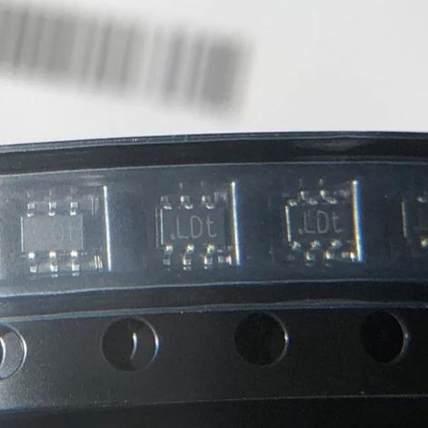
Image for reference only

Manufacturer Part:

NX3008CBKS,115

Package:

SOT363 (SC-88 / TSSOP-6), 6-Pin, 2.0mm × 1.25mm × 0.95mm

Brand:

Quality Commitment

Shipping & Payment

Service & Packaging

Product Manual

Description

Product Overview

The NX3008CBKS is a complementary N-channel and P-channel enhancement-mode Field-Effect Transistor (FET) pair from Nexperia, housed in a compact SOT363 (SC-88 / TSSOP-6) surface-mount package. Built on Trench MOSFET technology, this dual MOSFET features 30V drain-source voltage rating with 350mA continuous drain current for the N-channel device and 200mA for the P-channel device. With low threshold voltages of 0.9V typical and low on-resistance (1.4Ω N-channel @ 4.5V VGS), these devices are designed for logic-level drive applications. The NX3008CBKS is fully qualified to AEC-Q101 automotive standards, includes 2kV ESD protection, and offers very fast switching performance. Supplied in 7″ tape and reel packaging with 3,000 pieces per reel, it is ideal for level shifting, power supply converters, load switching, and general-purpose switching circuits in automotive and industrial applications.

Key Specifications

r>

Parameter N-Channel Value P-Channel Value
Manufacturer Nexperia
FET Type N-Channel Enhancement P-Channel Enhancement
Technology Trench MOSFET
VDS (Drain-Source Voltage) 30 V -30 V
VGS (Gate-Source Voltage) ±20 V ±20 V
ID Continuous Drain Current 350 mA -200 mA
ID (pulsed) 1.4 A -0.8 A
RDS(on) Max @ VGS=4.5V 1.4 Ω 2.5 Ω
RDS(on) Max @ VGS=2.5V 2.1 Ω 3.5 Ω
VGS(th) Gate Threshold (typ) 0.9 V -0.9 V
Gate Charge QG(tot) typ @4.5V 0.52 nC 0.44 nC
Gate-Drain Charge QGD typ 0.08 nC 0.07 nC
Input Capacitance Ciss typ 34 pF 25 pF
Output Capacitance Coss typ 6.5 pF 5.2 pF
Total Power Dissipation 280 mW (total package)
Operating Junction Temperature -55°C to +150°C
ESD Protection (gate-source) 2 kV (HBM)
Number of Transistors 2 (1 N-ch + 1 P-ch)
Qualification AEC-Q101 Automotive Grade
Package SOT363 (SC-88 / TSSOP-6), 6-pin
Package Dimensions 2.0mm × 1.25mm × 0.95mm
Marking LD%
Packaging Tape & Reel, 3,000 pcs/reel (7″ reel)

Features

  • Complementary N-channel and P-channel MOSFET pair
  • AEC-Q101 qualified for automotive applications
  • Trench MOSFET technology
  • Low threshold voltage: 0.9V typical
  • Very fast switching speed
  • Low gate charge: 0.52nC (N-ch), 0.44nC (P-ch)
  • 2kV ESD protection (gate-source HBM)
  • Logic-level gate drive compatible (2.5V and 4.5V)
  • Compact SOT363 (SC-88) package
  • Space-saving 6-lead TSSOP-6 form factor
  • Lead-free and RoHS compliant
  • Halogen-free and antimony-free
  • Wide operating temperature: -55°C to +150°C
  • Repetitive avalanche rated
  • Optimized for level shifter applications

Applications

  • Logic level shifting (3.3V ↔ 5V, 5V ↔ 12V)
  • Power supply converters and regulators
  • Load switching and power distribution
  • li>

  • General-purpose switching circuits
  • Automotive body electronics
  • Portable and battery-powered devices
  • Motor control and fan drives
  • LED backlight and display control
  • Signal switching and routing
  • Industrial control and automation
Product Introduction: NX3008CBKS,115 Product Introduction

The NX3008CBKS,115 from Nexperia is a complementary N-channel and P-channel enhancement-mode MOSFET pair in the ultra-compact SOT363 (SC-88) surface-mount package. Built on advanced Trench MOSFET technology, this dual device combines one N-channel and one P-channel MOSFET in a single 6-pin SOT363 package, making it ideal for complementary switching and level shifter applications where both N-channel and P-channel devices are needed. With a 30V drain-source voltage rating and 350mA / 200mA continuous drain current capability (N-channel / P-channel respectively), the NX3008CBK handles a wide range of low to medium power switching tasks. The low 0.9V typical threshold voltage enables direct drive from low-voltage logic circuits (2.5V and above), while the low gate charge (0.52nC N-channel, 0.44nC P-channel) enables high-speed switching with minimal drive requirements. Fully qualified to AEC-Q101 automotive standards with 2kV ESD protection on the gates, this device is suitable for the most demanding automotive and industrial environments. The 150°C maximum junction temperature rating provides ample thermal margin. The complementary N/P configuration in a single package reduces board space and component count compared to using two separate MOSFETs. Supplied in 7″ tape-and-reel packaging with 3,000 pieces per reel, the NX3008CBKS is widely used in logic level shifting, power supply converters, load switching, and general-purpose switching circuits.

Working Principle: NX3008CBKS,115 Working Principle

The NX3008CBKS contains two independent MOSFETs — one N-channel and one P-channel enhancement-mode Trench MOSFET — fabricated on a single silicon die and housed in a 6-pin SOT363 package. The N-channel MOSFET turns on when a positive voltage greater than the threshold voltage (VGS(th) = 0.9V typ) is applied between the gate and source, creating an n-type inversion layer that allows current to flow from drain to source. The P-channel MOSFET operates similarly but with opposite polarity — it turns on when the gate is driven negative relative to the source (VGS < -0.9V typ), allowing current to flow from source to drain. The Trench MOSFET technology creates vertical trench structures in the silicon, resulting in higher cell density, lower on-resistance, and faster switching compared to planar MOSFETs of equivalent die size. Both devices have the gate electrode electrically isolated from the channel by a thin silicon dioxide layer, giving them very high input impedance and near-zero DC gate current. The integrated 2kV ESD protection diodes on the gate terminals protect against electrostatic discharge during handling and assembly. In complementary pair applications (such as level shifters), the N-channel and P-channel devices work together — when the input is high, the N-channel turns on and the P-channel turns off, pulling the output low; when the input is low, the P-channel turns on and the N-channel turns off, pulling the output high. This push-pull configuration provides fast rise and fall times with low output impedance.

Pin Description: NX3008CBKS,115 Pin Definition and Functions
Pin Name Type Description
1 Drain P Power Drain of P-channel MOSFET
2 Gate P Input Gate of P-channel MOSFET
3 Source P Power Source of P-channel MOSFET
4 Source N Power Source of N-channel MOSFET
5 Gate N Input Gate of N-channel MOSFET
6 Drain N Power Drain of N-channel MOSFET

Marking: “LD%” (where % is the lot/batch code) is printed on the top surface of the SOT363 package. Pin 1 is identified by a beveled corner. Note that the N-channel and P-channel MOSFETs are independent devices with separate gate, source, and drain connections — they are not internally connected. The SOT363 package is also known as SC-88 or TSSOP-6, measuring just 2.0mm × 1.25mm × 0.95mm.

Application Scenarios: In which products and applications is NX3008CBKS,115 used
  • Logic Level Shifting: The complementary N/P configuration is ideal for bidirectional level shifting between different voltage domains (e.g., 3.3V to 5V, 1.8V to 3.3V) in mixed-voltage systems
  • Power Supply Converters: Used in low-power DC-DC converters, charge pumps, and inverting converters as the primary switching elements
  • Load Switching: Provides both high-side (P-channel) and low-side (N-channel) load switching capability in a single package for power distribution and management
  • Automotive Body Electronics: Deployed in BCM modules, door controllers, and lighting control units for signal switching and small load driving requiring AEC-Q101 qualification
  • LED Backlight Control: Implements PWM dimming control for LED backlights in displays, automotive instrument clusters, and lighting applications
  • Signal Switching: Used for analog and digital signal routing, multiplexing, and bus switching in communication and interface circuits
  • Battery-Powered Devices: Suitable for portable and battery-operated devices due to low threshold voltage, low gate charge, and support for low-voltage operation
  • Motor Control: Serves as the low-voltage control side of motor driver circuits, providing complementary drive signals for higher-power stages
Alternative Models: What chips are recommended as replacements for NX3008CBKS,115
Model Manufacturer Config VDS RDS(on) Package
NX3008PBK Nexperia N/P complementary 30V 1.4Ω/2.5Ω SOT363 (lead finish variant)
IRF7313 Infineon/IR N+P dual 30V 150mΩ/300mΩ SO-8
Si9928DY Vishay N+P dual 30V 45mΩ/80mΩ SO-8
ZVP4525GTA Diodes Inc P-ch only 250V 4.8Ω SOT-223
DMN601DWK Diodes Inc Dual N-ch 60V 2.5Ω SOT-363

Recommend Parts

ISL95855HRTZ-T

IMVP8 3+2+1 phase buck controller, R3 technology, 4.5-25V input, 48-TQFN

Brand: Renesas

Package: 48-TQFN (6×6 mm, exposed pad)

IN STOCK: 2156pcs

Cargo cycle: 3-7 Days

The minimum order is 1

IRFB4019PBF

150V N-Channel HEXFET Power MOSFET, 47A, 34 mΩ RDS(on), TO-220AB

Brand: infineon

Package: TO-220AB

IN STOCK: 2409pcs

Cargo cycle: 3-7 Days

The minimum order is 1

MSP430F247TPMR

TI MSP430 MCU, 16-bit RISC, 92KB Flash, 8KB RAM, 16MHz, LQFP-64

Package: See datasheet

IN STOCK: 13371pcs

Cargo cycle: 3-7 Days

The minimum order is 1

UCC28740DR

CVCC Flyback Controller, 700V startup, opto feedback, <10mW no-load, SOIC-7

Brand: TI

Package: SOIC-7 (4.9 x 3.9 x 1.75 mm)

IN STOCK: 4840pcs

Cargo cycle: 3-7 Days

The minimum order is 1

MMUN2211LT1G

NPN digital transistor, R1=10kΩ R2=10kΩ, 50V, 100mA, SOT-23-3, pre-biased BRT switch

Brand: Onsemi

Package: SOT-23-3 (TO-236, SC-59)

IN STOCK: 8500pcs

Cargo cycle: 3-7 Days

The minimum order is 1

PIC32MX795F512L-80I/PF

32-bit PIC32MX MCU with Ethernet/CAN/USB, 80MHz, 512KB Flash, TQFP-100, industrial

Brand: MICROCHIP

Package: TQFP-100 (14 x 14 mm)

IN STOCK: 7912pcs

Cargo cycle: 3-7 Days

The minimum order is 1





