






Opens in a new tab

Home » Integrated Circuits ICs, Logic Chips » LCMX02-640HC-4TG100T

LCMX02-640HC-4TG100T

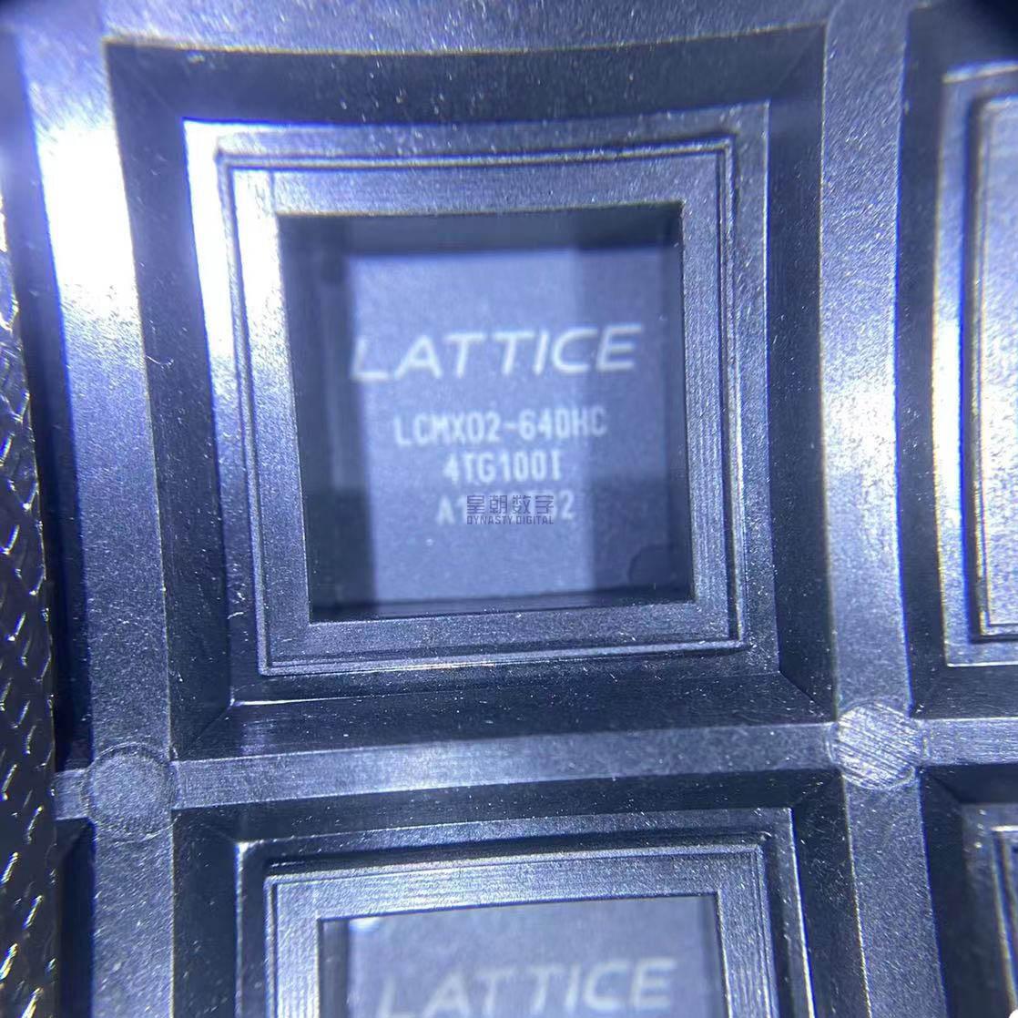
MachXO2 non-volatile FPGA, 640 LUTs, 78 I/O, 18kbit EBR, 100-TQFP

2057

Effective Inventory

Image for reference only

Manufacturer Part:

LCMX02-640HC-4TG100T

Package:

100-pin TQFP (14 x 14 x 1.4 mm, 0.5mm pitch, tray)

Brand:

Product Categories:

Quality Commitment

Shipping & Payment

Service & Packaging

Product Manual

Description

Product Overview

The LCMX02-640HC-4TG100T (MachXO2-640HC) is a low-power instant-on non-volatile FPGA from Lattice Semiconductor’s MachXO2 family. Featuring 640 Look-Up Tables (LUTs) of programmable logic, 78 user I/Os, 18 Kbit of embedded block RAM (EBR), and 5 Kbit of distributed RAM, this device is designed for low-cost, high-volume consumer and system applications. The MachXO2 architecture combines the flexibility of FPGAs with the instant-on, non-volatile nature of CPLDs. Built on a 65nm non-volatile low-power process, the device features embedded block RAM, distributed RAM, user flash memory (UFM), PLLs, and hardened versions of commonly used functions including SPI controller, I²C controller, and timer/counter. Packaged in a 100-pin TQFP, the MachXO2-640HC operates at speed grade 4 with commercial temperature range.

Key Specifications

Manufacturer Lattice Semiconductor
Product Type Non-volatile Low-Power FPGA (MachXO2)
Family MachXO2
Density 640 LUTs (Look-Up Tables)
Logic Cells 640
Number of LABs/CLBs 80
Embedded Block RAM (EBR) 18 Kbit (2 blocks × 9 Kbit)
Distributed RAM 5 Kbit
Total Memory ~23 Kbit
User Flash Memory (UFM) Yes
User I/O Pins 78
I/O Banks 4 banks
Differential I/O Pairs 39 (max)
Operating Supply Voltage 2.375 V to 3.6 V
I/O Voltage Standards 1.2V, 1.5V, 1.8V, 2.5V, 3.3V
Speed Grade 4
Max Operating Frequency 269 MHz
Operating Supply Current 1.84 mA (typ)
Operating Temperature 0°C to +85°C (commercial)
Package 100-pin TQFP (14 x 14 mm)
Programming JTAG, SPI flash, dual-boot
Status Active

Features

  • Ultra-low power, instant-on non-volatile FPGA
  • 640 LUTs, 78 I/O, 2.5V/3.3V operation
  • Embedded block RAM (EBR) and distributed RAM
  • User Flash Memory (UFM) for non-volatile data storage
  • PLLs for clock generation and management
  • Hardened SPI and I²C controller blocks
  • Built-in timer/counter peripheral
  • Pre-engineered source synchronous I/O support
  • Advanced configuration with dual-boot capability
  • TransFR™ reconfiguration technology
  • Programmable low-swing differential I/Os
  • Dynamic power management (I/O banks, PLLs, oscillators)
  • 65nm non-volatile low-power process technology

Applications

  • Consumer electronics and portable devices
  • System control and management functions
  • Board-level glue logic and interface bridging
  • Power sequencing and system initialization
  • Industrial control and monitoring
  • Display control and timing
  • Communication interfaces and protocol bridging
  • Cost-sensitive high-volume applications

Product Introduction: LCMX02-640HC-4TG100T Product Introduction

The LCMX02-640HC-4TG100T (MachXO2-640HC) from Lattice Semiconductor is an ultra-low power, instant-on non-volatile FPGA belonging to the MachXO2 family. Designed for low-cost, high-volume consumer and system applications, this device combines the flexibility and breadth of FPGA resources with the instant-on, non-volatile characteristics traditionally associated with CPLDs. Built on a 65nm non-volatile low-power process technology, the MachXO2-640HC features 640 Look-Up Tables (LUTs) of programmable logic, 18 Kbit of embedded block RAM (EBR) organized as two 9 Kbit blocks, 5 Kbit of distributed RAM, and User Flash Memory (UFM) for non-volatile data storage. The device provides 78 user I/O pins across four I/O banks, supporting multiple I/O standards including LVTTL, LVCMOS (1.2V, 1.5V, 1.8V, 2.5V, 3.3V), and LVDS. Pre-engineered hardened IP blocks include an SPI controller, I²C controller, and timer/counter, reducing design effort for common interface functions. PLLs provide flexible clock generation and management. The device supports advanced configuration features including dual-boot capability and TransFR™ (Transparent Field Reconfiguration) technology, allowing reconfiguration without interrupting system operation. With a 1.84mA typical operating supply current and ultra-low standby power, the MachXO2-640HC is ideal for battery-powered and energy-sensitive applications. Available in a 100-pin TQFP package with commercial temperature grade (0°C to 85°C), speed grade 4, this device is well-suited for consumer electronics, industrial control, system management, glue logic, and cost-sensitive high-volume applications.

Working Principle: LCMX02-640HC-4TG100T Working Principle

The LCMX02-640HC operates as a non-volatile FPGA with embedded memory and hardened IP blocks. Its architectural framework includes: 1) Programmable Logic Array: 640 4-input Look-Up Tables (LUTs) organized into 80 Logic Array Blocks (LABs) provide the core programmable logic fabric. Each LUT can implement any 4-input combinational function, and can also be configured as distributed RAM or shift register. Flip-flops associated with each LUT support registered or combinatorial outputs. 2) Embedded Block RAM (EBR): Two 9 Kbit embedded block RAM blocks provide true dual-port memory for data buffering, FIFO implementation, and general-purpose data storage. EBR can be configured in various widths and depths, including single-port, dual-port, and FIFO modes. 3) User Flash Memory (UFM): Non-volatile flash memory stores user data, configuration settings, or calibration coefficients. UFM retains data through power cycles and can be accessed via the user logic design. 4) Hardened IP Blocks: Hardened (silicon-proven, non-LUT) peripheral blocks include an SPI controller, I²C controller, and timer/counter. These are accessed through the internal system bus and provide efficient implementation of common interface functions without consuming LUT resources. 5) Clock Management: PLLs generate precise clock frequencies from reference clock inputs, supporting clock multiplication, division, and phase shifting. Multiple clock domains are supported for complex timing requirements. 6) I/O Structure: Four I/O banks with independent supply voltages support multiple I/O standards. Programmable low-swing differential I/Os are available. Each I/O pin includes input and output registers, programmable pull-up/pull-down, and slew rate control. 7) Configuration Memory: Non-volatile configuration memory stores the FPGA programming data. On power-up, the configuration is loaded into SRAM-based programming latches, providing instant-on operation. JTAG, SPI, and dual-boot configuration options are supported.

Pin Description: LCMX02-640HC-4TG100T Pin Definition and Functions
Pin Category Function Description
VCC (Core) Core Power Core supply voltage (2.375V to 3.465V, internally regulated)
VCCIO0-3 I/O Bank Power I/O bank supply voltages (4 banks, independent)
GND Ground Multiple ground pins for power and signal integrity
I/O Bank Pins User I/O 78 user I/O pins across 4 banks (Bank 0, 1, 2, 3)
JTAG Pins TCK, TMS, TDI, TDO JTAG test access port for programming and boundary scan
Clock Pins Global Clock Inputs Dedicated clock input pins (can also be used as I/O)
PLL Pins PLL_REF, PLL_OUT PLL reference clock and output pins
Configuration Pins CRESET, CDONE, etc. FPGA configuration reset and status pins
SPI Pins SPI_SCK, SPI_MISO, etc. SPI configuration interface pins
Application Scenarios: In which products and applications is LCMX02-640HC-4TG100T used
  • Consumer electronics power management and system control
  • Board-level glue logic and bus bridging in embedded systems
  • Power sequencing, reset generation, and system initialization
  • Display panel timing control and interface conversion
  • Industrial sensor interfaces and control logic
  • Communication protocol bridging and interface translation
  • Cost-sensitive high-volume IoT and consumer devices
  • Handheld and battery-powered portable electronics
Alternative Models: What chips are recommended as replacements for LCMX02-640HC-4TG100T
Manufacturer Part Number LUTs Package Notes
Lattice LCMXO2-1200HC 1200 100-TQFP Higher density, same package
Lattice LCMXO2-256HC 256 100-TQFP Lower density version
Lattice LCMXO2-640ZE 640 WLCSP Ultra-low power, small package
Microchip IGLOO2 M2GL005 4800 Various Flash-based FPGA, higher density
Xilinx Spartan-7 XC7S6 6800 CPGA196 SRAM-based FPGA, needs config memory

Recommend Parts

ISL95855HRTZ-T

IMVP8 3+2+1 phase buck controller, R3 technology, 4.5-25V input, 48-TQFN

Brand: Renesas

Package: 48-TQFN (6×6 mm, exposed pad)

IN STOCK: 2156pcs

Cargo cycle: 3-7 Days

The minimum order is 1

IRFB4020PBF

200V N-Channel HEXFET Power MOSFET, 31A, 68 mΩ RDS(on), TO-220AB

Brand: infineon

Package: TO-220AB

IN STOCK: 14149pcs

Cargo cycle: 3-7 Days

The minimum order is 1

NRF52832-QFAA-T

Nordic BLE SoC, ARM Cortex-M4 @ 64MHz, 64KB Flash, 32KB RAM, QFN-48

Package: See datasheet

IN STOCK: 10958pcs

Cargo cycle: 3-7 Days

The minimum order is 1

UCC28740DR

CVCC Flyback Controller, 700V startup, opto feedback, <10mW no-load, SOIC-7

Brand: TI

Package: SOIC-7 (4.9 x 3.9 x 1.75 mm)

IN STOCK: 4840pcs

Cargo cycle: 3-7 Days

The minimum order is 1

MMUN2211LT1G

NPN digital transistor, R1=10kΩ R2=10kΩ, 50V, 100mA, SOT-23-3, pre-biased BRT switch

Brand: Onsemi

Package: SOT-23-3 (TO-236, SC-59)

IN STOCK: 8500pcs

Cargo cycle: 3-7 Days

The minimum order is 1

PIC32MX795F512L-80I/PF

32-bit PIC32MX MCU with Ethernet/CAN/USB, 80MHz, 512KB Flash, TQFP-100, industrial

Brand: MICROCHIP

Package: TQFP-100 (14 x 14 mm)

IN STOCK: 7912pcs

Cargo cycle: 3-7 Days

The minimum order is 1




