






Opens in a new tab

Home » Integrated Circuits ICs, Logic Chips » LCMXO256C-4TN100C-3I

LCMXO256C-4TN100C-3I

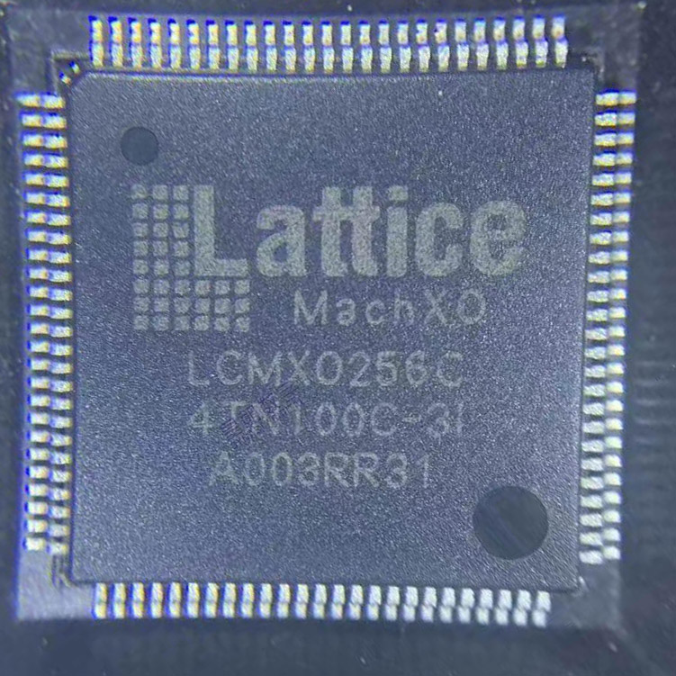
MachXO crossover PLD, 256 LUTs, 78 I/O, non-volatile, 100-TQFP

1689

Effective Inventory

Image for reference only

Manufacturer Part:

LCMXO256C-4TN100C-3I

Package:

100-pin TQFP (14 x 14 mm, 0.5mm pitch, commercial grade)

Brand:

Product Categories:

Quality Commitment

Shipping & Payment

Service & Packaging

Product Manual

Description

Product Overview

The LCMXO256C-4TN100C-3I is a non-volatile Crossover PLD from Lattice Semiconductor’s MachXO family. Featuring 256 LUTs and 78 user I/Os, this device combines the advantages of CPLDs (instant-on, low cost) with the density and features of FPGAs (embedded memory, PLLs, flexible I/O). Built on a 130nm non-volatile process, the MachXO256C provides 256 Look-Up Tables, 78 I/O pins, 2048 bits of distributed RAM, and 192 registers. With a 3.3V core supply and support for multiple I/O standards (LVTTL, LVCMOS, PCI, LVDS), the device operates at speed grade 4 with 4.2ns propagation delay. The 100-pin TQFP commercial-grade device provides a flexible solution for system-level glue logic, bus bridging, and control applications.

Key Specifications

Manufacturer Lattice Semiconductor
Product Type Crossover PLD / CPLD
Family MachXO
Density 256 LUTs (Look-Up Tables)
Number of LABs/CLBs 32
Macrocells 128
Registers 192
Total Memory (Distributed) 2048 bits
User I/O Pins 78
I/O Banks 2 banks
Operating Voltage (Core) 1.71 V to 3.465 V (1.8V/2.5V/3.3V)
I/O Standards LVTTL, LVCMOS 3.3V/2.5V/1.8V/1.5V/1.2V, LVDS, PCI
Speed Grade 4
Propagation Delay 4.2 ns (typical)
Maximum Frequency 156.25 MHz
Operating Supply Current 13 mA (typical)
Programmability In-system programmable (JTAG)
Configuration Memory Non-volatile flash
Operating Temperature 0°C to +85°C (commercial)
Package 100-pin TQFP (14 x 14 mm)
Global Clocks 8

Features

  • 256 LUTs, 78 I/O, crossover PLD architecture
  • Instant-on, non-volatile flash configuration
  • Wide operating voltage range: 1.71V to 3.465V
  • Multiple I/O standards: LVTTL, LVCMOS, LVDS, PCI
  • Distributed RAM (2048 bits)
  • 8 global clock networks
  • In-system programmability via JTAG
  • Reprogrammable (infinitely reconfigurable)
  • Programmable output slew rate
  • Pin-locking capability for design iterations
  • Two I/O banks with independent voltage supplies
  • RoHS compliant and lead-free package

Applications

  • System glue logic and interface bridging
  • Bus interfaces and address decoding
  • Power-up sequencing and reset generation
  • Configuration management and control logic
  • State machines and control paths
  • Display timing and control circuits
  • Consumer and industrial electronics
  • FPGA/ASIC configuration and control

Product Introduction: LCMXO256C-4TN100C-3I Product Introduction

The LCMXO256C-4TN100C-3I is a MachXO family Crossover Programmable Logic Device (PLD) from Lattice Semiconductor. As a crossover PLD, the MachXO family bridges the gap between traditional CPLDs and FPGAs, combining CPLD-like features (instant-on, non-volatile, low cost, pin-locking) with FPGA-like capabilities (higher density, embedded memory, flexible I/O standards, PLLs on higher densities). The LCMXO256C features 256 Look-Up Tables (LUTs) of programmable logic, 128 macrocells, 192 registers, 78 user I/O pins, and 2048 bits of distributed RAM. With a wide core operating voltage range of 1.71V to 3.465V and support for multiple I/O standards including LVTTL, LVCMOS (3.3V/2.5V/1.8V/1.5V/1.2V), LVDS, and PCI, the device provides excellent interface flexibility for mixed-voltage systems. Eight global clock networks support complex multi-clock designs. Non-volatile flash memory provides instant-on operation (no external configuration ROM needed) and in-system programmability via the standard JTAG interface. Pin-locking capability allows design modifications without changing the PCB layout. Available in a 100-pin TQFP package at speed grade 4 with commercial temperature range (0°C to 85°C), the LCMXO256C is ideal for system-level glue logic, bus interfacing, power sequencing, configuration management, and other control-oriented applications in consumer, industrial, and communication systems.

Working Principle: LCMXO256C-4TN100C-3I Working Principle

The LCMXO256C operates as a non-volatile crossover PLD combining FPGA-style logic fabric with CPLD-like instant-on operation. Its functional architecture includes: 1) Logic Array Blocks (LABs): 32 LABs each containing 8 LUTs (total 256 LUTs) form the core logic fabric. Each 4-input LUT can implement any combinatorial function of four variables. Associated flip-flops can be configured as D, T, JK, or SR registers. LABs are interconnected through a global routing pool. 2) Distributed RAM: LUTs can be configured as distributed RAM (2048 bits total), providing small on-chip memory for data buffers, FIFOs, and shift registers without consuming dedicated block RAM resources. 3) I/O Banks: Two I/O banks with independent supply voltages support a variety of I/O standards. Each I/O pin includes an input register, output register, output enable, and programmable pull-up/down. Slew rate control helps manage signal integrity and EMI. LVDS differential I/O pairs support high-speed serial interfaces. 4) Clock Network: Eight global clock networks distribute clocks throughout the device with low skew. Multiple clock domains are supported for complex multi-clock designs. Clock pins can also be used as general I/O when not needed for clocking. 5) Non-Volatile Configuration: Flash-based non-volatile configuration memory stores the programmed design. On power-up, configuration data is loaded into the SRAM programming latches, providing instant-on operation. In-system programming via JTAG allows field updates. TransFR technology enables transparent reconfiguration while maintaining I/O states.

Pin Description: LCMXO256C-4TN100C-3I Pin Definition and Functions
Pin Category Description
VCC (Core) Core logic supply voltage (1.71V to 3.465V)
VCCIO0, VCCIO1 I/O bank 0 and bank 1 supply voltages (independent)
GND Ground pins (multiple for power distribution)
I/O Bank 0 Pins User I/O pins in bank 0 (LVDS pairs, single-ended)
I/O Bank 1 Pins User I/O pins in bank 1 (LVDS pairs, single-ended)
JTAG TCK (clock), TMS (mode select), TDI (data in), TDO (data out)
Global Clock Pins 8 dedicated global clock inputs (can be used as I/O)
Configuration Pins Dedicated configuration pins (if applicable)
Application Scenarios: In which products and applications is LCMXO256C-4TN100C-3I used
  • System glue logic for embedded and computer systems
  • Bus interface bridging and protocol translation
  • Address decoding and chip select generation
  • Power-up sequencing and system reset generation
  • FPGA/ASIC configuration control and boot sequence management
  • Display panel timing and control circuits
  • Industrial control and monitoring logic
  • Consumer electronics system management
Alternative Models: What chips are recommended as replacements for LCMXO256C-4TN100C-3I
Manufacturer Part Number LUTs Package Notes
Lattice LCMXO256C-4TN100I 256 100-TQFP Industrial temp (-40°C to 100°C)
Lattice LCMXO640C-4TN100C 640 100-TQFP Higher density, same package
Lattice LCMXO2-256HC 256 100-TQFP MachXO2 generation, more features
Xilinx (AMD) XC95288XL 288 MC 100-TQFP 3.3V CPLD, 288 macrocells
Altera (Intel) EPM570T100C5N 570 LE 100-TQFP MAX II family, higher density

Recommend Parts

ISL95855HRTZ-T

IMVP8 3+2+1 phase buck controller, R3 technology, 4.5-25V input, 48-TQFN

Brand: Renesas

Package: 48-TQFN (6×6 mm, exposed pad)

IN STOCK: 2156pcs

Cargo cycle: 3-7 Days

The minimum order is 1

IRFB4020PBF

200V N-Channel HEXFET Power MOSFET, 31A, 68 mΩ RDS(on), TO-220AB

Brand: infineon

Package: TO-220AB

IN STOCK: 14149pcs

Cargo cycle: 3-7 Days

The minimum order is 1

NRF52832-QFAA-T

Nordic BLE SoC, ARM Cortex-M4 @ 64MHz, 64KB Flash, 32KB RAM, QFN-48

Package: See datasheet

IN STOCK: 10958pcs

Cargo cycle: 3-7 Days

The minimum order is 1

UCC28740DR

CVCC Flyback Controller, 700V startup, opto feedback, <10mW no-load, SOIC-7

Brand: TI

Package: SOIC-7 (4.9 x 3.9 x 1.75 mm)

IN STOCK: 4840pcs

Cargo cycle: 3-7 Days

The minimum order is 1

MMUN2211LT1G

NPN digital transistor, R1=10kΩ R2=10kΩ, 50V, 100mA, SOT-23-3, pre-biased BRT switch

Brand: Onsemi

Package: SOT-23-3 (TO-236, SC-59)

IN STOCK: 8500pcs

Cargo cycle: 3-7 Days

The minimum order is 1

PIC32MX795F512L-80I/PF

32-bit PIC32MX MCU with Ethernet/CAN/USB, 80MHz, 512KB Flash, TQFP-100, industrial

Brand: MICROCHIP

Package: TQFP-100 (14 x 14 mm)

IN STOCK: 7912pcs

Cargo cycle: 3-7 Days

The minimum order is 1




