






Opens in a new tab

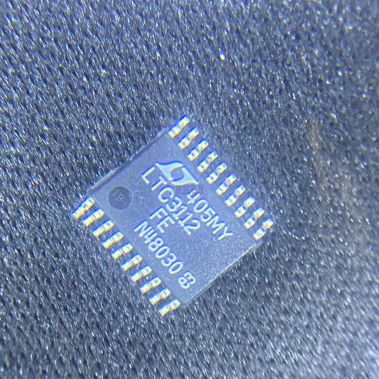
LTC3112EFE

2.5A Synchronous Buck-Boost Converter, 2.7V-40V In, 1V-38V Out, TSSOP-20

12077

Effective Inventory

Image for reference only

Manufacturer Part:

LTC3112EFE

Package:

TSSOP-20, 6.5 x 4.4 x 1.0 mm

Brand:

Quality Commitment

Shipping & Payment

Service & Packaging

Product Manual

Description

Product Overview

The LTC3112EFE is a high-efficiency 2.5A synchronous buck-boost DC-DC converter from Analog Devices, capable of operating from input voltages above, below, or equal to the output voltage. With a wide 2.7V to 40V input range and 1V to 38V adjustable output, this device is ideal for battery-powered applications where the input voltage varies across the output voltage level (e.g., single-cell Li-ion to 3.3V, or multi-cell alkaline to 5V). Synchronous rectification delivers efficiencies up to 95%, while Burst Mode® operation reduces quiescent current to just 35µA for extended battery life. The TSSOP-20 package provides a compact solution for industrial, automotive, solar-powered, and battery-powered systems.

Key Specifications

Parameter Value
Manufacturer Analog Devices
Part Number LTC3112EFE
Product Category Synchronous Buck-Boost Converters
Topology 4-Switch Buck-Boost (SEPIC alternative)
Input Voltage Range 2.7V to 40V
Output Voltage Range 1V to 38V (adjustable)
Output Current 2.5A continuous (buck mode, VIN=12V, VOUT=5V)
Switching Frequency 100kHz to 2MHz (programmable)
Peak Efficiency Up to 95% (synchronous rectification)
Quiescent Current 35µA (Burst Mode operation)
Package / Case TSSOP-20
Operating Temperature -40°C to +125°C

Features

  • Wide 2.7V to 40V input voltage range
  • Wide 1V to 38V output voltage range
  • 2.5A continuous output current (buck mode conditions)
  • Synchronous rectification: up to 95% efficiency
  • Programmable switching frequency: 100kHz to 2MHz
  • Burst Mode operation: 35µA quiescent current for light loads
  • Seamless transitions between buck, boost, and buck-boost modes
  • Programmable soft-start
  • Output disconnect during shutdown
  • Thermal overload and short-circuit protection
  • TSSOP-20 package with exposed pad for thermal performance

Applications

  • Industrial and automotive power supplies
  • Battery-powered instruments and handheld devices
  • Distributed power systems and intermediate buses
  • Solar-powered systems and energy harvesting
  • High-power LED drivers
  • Single-/multi-cell battery to 3.3V/5V/12V conversion

Product Introduction: LTC3112EFE Product Introduction

The LTC3112EFE is a high-performance synchronous buck-boost DC-DC converter from Analog Devices, designed for applications where the input voltage can be above, below, or equal to the output voltage. This makes it ideal for battery-powered systems where the battery discharge curve crosses the desired output voltage, such as a single Li-ion cell (2.7V-4.2V) powering a 3.3V system, or a 12V automotive supply (9V-16V) regulating a 12V output.

The LTC3112 uses a four-switch (two high-side, two low-side) synchronous buck-boost topology that provides seamless transitions between buck mode (VIN > VOUT), boost mode (VIN < VOUT), and buck-boost mode (VIN ≈ VOUT). Unlike SEPIC or flyback topologies, the four-switch buck-boost uses a single inductor and provides high efficiency across all operating modes.

Synchronous rectification (both high-side and low-side switches are MOSFETs, not diodes) delivers high efficiency up to 95%. For light-load efficiency, Burst Mode operation reduces quiescent current to just 35µA, significantly extending battery life in always-on systems. The switching frequency is programmable from 100kHz to 2MHz via a single resistor, allowing optimization between component size and efficiency.

Additional features include programmable soft-start to limit inrush current, output disconnect during shutdown (prevents battery drain through the output), and comprehensive protection including thermal shutdown, overcurrent protection, and short-circuit protection. The TSSOP-20 package with exposed pad provides good thermal dissipation for reliable operation at high power levels.

Working Principle: LTC3112EFE Working Principle

The LTC3112 is a four-switch synchronous buck-boost converter operating as follows:

1. Four-Switch Topology: The converter uses four MOSFETs: two high-side (A and B) and two low-side (C and D), arranged around a single inductor. Switch A connects VIN to the inductor, switch D connects the inductor to ground (input side). Switch B connects VOUT to the inductor, switch C connects the inductor to ground (output side). This allows operation in buck, boost, and buck-boost modes.

2. Buck Mode (VIN > VOUT): In buck mode, switches B and C form the buck pair on the output side. Switch A is always on, switch D is always off. B and C switch alternately like a standard buck converter, stepping down the voltage.

3. Boost Mode (VIN < VOUT): In boost mode, switches A and D form the boost pair on the input side. Switch B is always on, switch C is always off. A and D switch alternately like a standard boost converter, stepping up the voltage.

4. Buck-Boost Mode (VIN ≈ VOUT): When input and output voltages are close, all four switches operate in a combined sequence that maintains regulation through the transition region. This ensures seamless mode transitions without glitches or excessive output ripple.

5. Control Architecture: The LTC3112 uses current-mode control with an inner current loop and outer voltage loop. The error amplifier compares the feedback voltage against a 0.8V reference and sets the peak inductor current. This provides good line and load regulation plus inherent cycle-by-cycle current limiting.

6. Burst Mode Operation: At light loads, the converter enters Burst Mode. It delivers short bursts of current to the output, then shuts down most of the control circuitry for extended periods. This reduces the average quiescent current to 35µA, maximizing efficiency at low output currents.

7. Protection Features: Cycle-by-cycle current limit on both switches, output overvoltage protection, thermal shutdown, and output disconnect (prevents reverse current when shut down).

Pin Description: LTC3112EFE Pin Definition and Functions
Pin Name Type Description
1 SW1 I/O Switch node 1 (input side). Connect to one end of inductor and drain of switch A / source of switch D.
2 VIN Power Input Input voltage supply (2.7V to 40V). Bypass with ceramic capacitors to GND.
3 VIN Power Input Second VIN pin. Connected internally. Both pins must be connected together.
4 RUN Input Run / enable input. Drive above 1.2V to enable. Pull below 0.5V to shut down.
5 FB Input Feedback input. Connect resistor divider from VOUT to FB to GND. Regulation point = 0.8V.
6 ISET Input Current limit programming. Resistor to GND sets peak switch current limit.
7 RT Input Oscillator frequency programming. Resistor to GND sets switching frequency (100kHz to 2MHz).
8 SS I/O Soft-start pin. Connect capacitor to GND to program soft-start time. Limits inrush current during start-up.
9 SYNC/MODE Input Synchronization / mode select. External clock input for sync, or tie to GND/VCC for Burst Mode/pulse-skipping selection.
10 GND Ground Signal ground. Connect to ground plane.
11 PG Output Power-good open-drain output. Flags when VOUT is within regulation. Requires external pull-up.
12 CLKOUT Output Clock output. 180° out-of-phase clock for driving additional converters in multiphase designs.
13 GND Ground Power ground. Return path for high-current switching.
14 GND Ground Second power ground pin.
15 VOUT Output Output voltage sense. Connect to VOUT rail for output voltage sensing.
16 VOUT Output Output power. Connect to output capacitors and load.
17 SW2 I/O Switch node 2 (output side). Connect to other end of inductor and drain of switch B / source of switch C.
18 SW2 I/O Second SW2 pin. Connected internally. Both pins connected together externally.
19 GND Ground Additional power ground pin.
20 GND Ground Additional power ground pin.
Pad EP Thermal Exposed pad. Solder to ground plane with multiple vias for thermal dissipation.
Application Scenarios: In which products and applications is LTC3112EFE used
  • Battery-powered instruments (Li-ion to 3.3V / 5V)
  • Automotive 12V systems with cold-crank and load-dump conditions
  • Industrial 24V to 12V/5V/3.3V power supplies
  • Solar-powered sensor nodes and energy harvesting
  • High-power LED drivers with wide input voltage range
  • Distributed power architectures with variable input
Alternative Models: What chips are recommended as replacements for LTC3112EFE
Manufacturer Part Number Package Notes
Analog Devices LTC3115-1 DFN-12 2A 2.7V-40V buck-boost
Analog Devices LTC3780 SSOP-28 Controller version (external FETs, higher power)
Analog Devices LTC3533 DFN 2.4V-15V, 200mA lower power
Texas Instruments LM5175 QFN-28 4-switch buck-boost controller
Texas Instruments TPS63070 QFN-15 2A 2V-16V buck-boost
MPS MP8869 QFN 3A buck-boost alternative

Recommend Parts

ISO1176TDWR

Isolated RS-485 transceiver, 40Mbps, integrated transformer driver, SOIC-16

Brand: TI

Package: SOIC-16 (DW, wide-body, 10.3 x 10.3 mm)

IN STOCK: 6874pcs

Cargo cycle: 3-7 Days

The minimum order is 1

IRFB4020PBF

200V N-Channel HEXFET Power MOSFET, 31A, 68 mΩ RDS(on), TO-220AB

Brand: infineon

Package: TO-220AB

IN STOCK: 14149pcs

Cargo cycle: 3-7 Days

The minimum order is 1

NRF52832-QFAA-T

Nordic BLE SoC, ARM Cortex-M4 @ 64MHz, 64KB Flash, 32KB RAM, QFN-48

Package: See datasheet

IN STOCK: 10958pcs

Cargo cycle: 3-7 Days

The minimum order is 1

UCC28740DR

CVCC Flyback Controller, 700V startup, opto feedback, <10mW no-load, SOIC-7

Brand: TI

Package: SOIC-7 (4.9 x 3.9 x 1.75 mm)

IN STOCK: 4840pcs

Cargo cycle: 3-7 Days

The minimum order is 1

MMUN2211LT1G

NPN digital transistor, R1=10kΩ R2=10kΩ, 50V, 100mA, SOT-23-3, pre-biased BRT switch

Brand: Onsemi

Package: SOT-23-3 (TO-236, SC-59)

IN STOCK: 8500pcs

Cargo cycle: 3-7 Days

The minimum order is 1

PIC32MX795F512L-80I/PF

32-bit PIC32MX MCU with Ethernet/CAN/USB, 80MHz, 512KB Flash, TQFP-100, industrial

Brand: MICROCHIP

Package: TQFP-100 (14 x 14 mm)

IN STOCK: 7912pcs

Cargo cycle: 3-7 Days

The minimum order is 1




