






Opens in a new tab

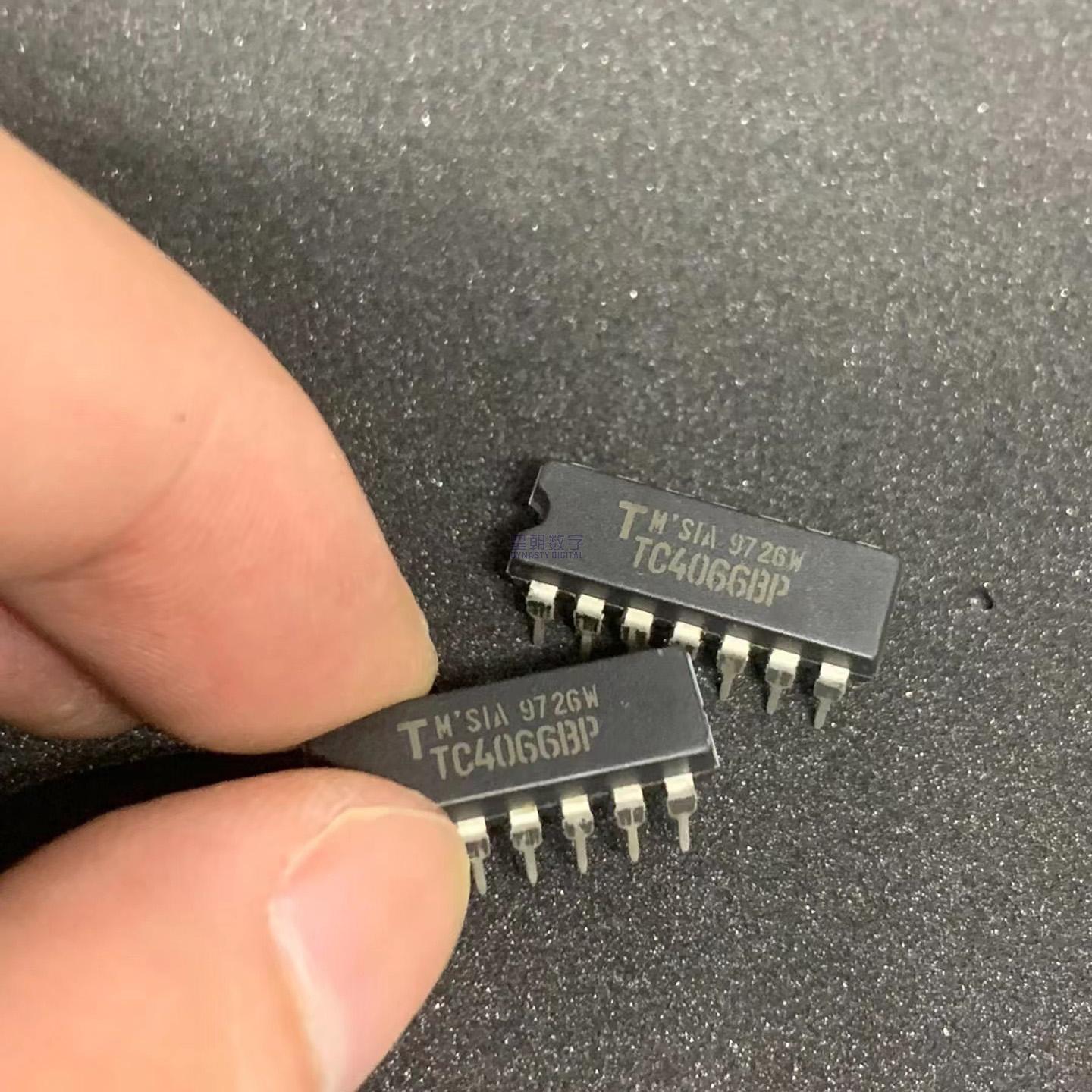
TC4066BP

Quad bilateral analog switch, 3-18V supply, 250Ω@5V Ron, 4 circuits, DIP-14, Toshiba CMOS logic

15400

Effective Inventory

Image for reference only

Manufacturer Part:

TC4066BP

Package:

DIP-14 (19.75 x 7.62 mm, through-hole)

Brand:

Quality Commitment

Shipping & Payment

Service & Packaging

Product Manual

Description

Product Overview

The TC4066BP is a quad bilateral (bidirectional) analog switch from Toshiba’s standard CMOS logic family, providing four independent SPST (Single-Pole Single-Throw) switch circuits in a single 14-pin DIP package. Each switch conducts bidirectionally when its control input is high and blocks when low, with the ability to pass both analog and digital signals. Built on CMOS technology, it features low on-resistance (250 Ω typ. at 5 V, 70 Ω typ. at 15 V), very high off-resistance (>1 GΩ), and low power consumption typical of CMOS devices. The wide operating voltage range of 3 V to 18 V accommodates various system levels, and the standard 4000-series pinout ensures broad compatibility. The through-hole DIP-14 package makes it well-suited for prototyping, breadboarding, and applications where through-hole construction is preferred.

Key Specifications

Type Quad Bilateral Analog Switch (SPST)
Technology CMOS (Standard 4000 series)
Number of Switches 4 independent channels
Supply Voltage Range 3 V to 18 V
On-Resistance (Ron) 250 Ω typ. @ VDD=5V
On-Resistance (Ron) 110 Ω typ. @ VDD=10V
On-Resistance (Ron) 70 Ω typ. @ VDD=15V
Off-Resistance (Roff) > 1 GΩ typ.
Ron Matching (between switches) 10 Ω typ. @ VDD=5V
Propagation Delay (tpd_tpz) 5 ns typ. @ VDD=15V
Control Input High (VIH) 3.5 V min. @ VDD=5V
Control Input Low (VIL) 1.5 V max. @ VDD=5V
Signal Range 0 V to VDD
Power Dissipation 300 mW max. (DIP package)
Operating Temperature -40°C to +85°C
Package DIP-14 (through-hole, 2.54mm pitch)

Features

  • 4 independent bilateral (bidirectional) switches
  • CMOS transmission gate structure (NMOS + PMOS parallel)
  • Low on-resistance: 70-250 Ω (depending on VDD)

Very high off-isolation: > 1 GΩ

  • Wide supply voltage range: 3 V to 18 V
  • Low power consumption (CMOS)
  • Bidirectional signal flow (analog or digital)
  • Matched switch characteristics between channels
  • Standard 4000-series CMOS equivalent (CD4066B)
  • High noise immunity
  • -40°C to +85°C industrial temperature range
  • Through-hole DIP-14 package
  • RoHS compliant, lead-free
  • Low cost, general-purpose switch solution

Applications

  • Analog signal switching and routing
  • Digital signal multiplexing and demultiplexing
  • Audio and video signal selector circuits
  • Data acquisition and sample-hold systems
  • Chopper, modulator, and demodulator circuits
  • Analog multiplexer/demultiplexer designs
  • Function generators and test equipment
  • Industrial control and automation
  • Prototyping, breadboarding, and education
  • Communication systems signal paths

Product Introduction: TC4066BP Product Introduction

The TC4066BP is a quad bilateral switch from Toshiba’s standard CMOS logic series, containing four independent bidirectional analog switch circuits. When the control input (CONT) is set to high level, the impedance between the input and output of each switch becomes low (conducting state), and when set to low level, the impedance becomes very high (off state). The device can be used for switching both analog signals and digital signals, with on-resistance as low as 70 Ω typical at VDD-VSS = 15 V and off-resistance exceeding 1 GΩ. Operated from a single 3 V to 18 V supply, the TC4066BP is a versatile 4000-series CMOS equivalent to the CD4066B, suitable for signal switching, multiplexing, chopper, and modulator/demodulator applications. Packaged in a through-hole DIP-14 format, it is widely used in prototyping, industrial, and consumer electronics.

Working Principle: TC4066BP Working Principle

The TC4066BP implements each bilateral switch using a transmission gate structure consisting of parallel NMOS and PMOS transistors. When the control terminal is high (near VDD), both transistors conduct, creating a low-resistance bidirectional path between the input and output terminals. The parallel combination of NMOS and PMOS ensures low on-resistance across the full signal swing range from VSS to VDD, avoiding the voltage drop issues of a single-transistor pass gate. When the control terminal is low (near VSS), both transistors are cut off, providing extremely high isolation (>1 GΩ) between the signal terminals. The bidirectional nature means each switch terminal can serve as either input or output depending on signal direction. Each of the four switches operates independently. The CMOS construction provides low power consumption and high noise immunity, while the wide 3 V to 18 V supply range accommodates both low-voltage and higher-voltage analog signal switching applications.

Pin Description: TC4066BP Pin Definition and Functions
Pin No. Pin Name Description
1 I/O A (Switch 1) Bidirectional I/O terminal for switch 1
2 O/I A (Switch 1) Bidirectional I/O terminal for switch 1
3 I/O B (Switch 2) Bidirectional I/O terminal for switch 2
4 O/I B (Switch 2) Bidirectional I/O terminal for switch 2
5 Control B Control input for switch 2
6 Control C Control input for switch 3
7 VSS Ground (negative supply)
8 I/O C (Switch 3) Bidirectional I/O terminal for switch 3
9 O/I C (Switch 3) Bidirectional I/O terminal for switch 3
10 I/O D (Switch 4) Bidirectional I/O terminal for switch 4
11 O/I D (Switch 4) Bidirectional I/O terminal for switch 4
12 Control D Control input for switch 4
13 Control A Control input for switch 1
14 VDD Positive power supply

Truth Table: Control = H → Switch ON (low impedance); Control = L → Switch OFF (high impedance)

Application Scenarios: In which products and applications is TC4066BP used
  • Analog signal switching and routing
  • Digital signal multiplexing/demultiplexing
  • Audio and video signal switching
  • Data acquisition and sample-and-hold circuits
  • Chopper and modulator/demodulator circuits
  • Analog multiplexers and mux/demux systems
  • Function generators and test equipment
  • Industrial control and automation
  • Prototyping and breadboard circuits
Alternative Models: What chips are recommended as replacements for TC4066BP
Model Channels Package Description
TC4066BF 4 SOP14 Surface mount version, same specs
CD4066B 4 DIP14/SOP14 TI/NS equivalent (same pinout)
HEF4066B 4 DIP14 Nexperia equivalent
DG4088 8 SOP16 8-channel single-pole switch
ADG1419 4 LFCSP High-performance, low Ron alternative

Recommend Parts

ISO1176TDWR

Isolated RS-485 transceiver, 40Mbps, integrated transformer driver, SOIC-16

Brand: TI

Package: SOIC-16 (DW, wide-body, 10.3 x 10.3 mm)

IN STOCK: 6874pcs

Cargo cycle: 3-7 Days

The minimum order is 1

IRFB4020PBF

200V N-Channel HEXFET Power MOSFET, 31A, 68 mΩ RDS(on), TO-220AB

Brand: infineon

Package: TO-220AB

IN STOCK: 14149pcs

Cargo cycle: 3-7 Days

The minimum order is 1

NRF52832-QFAA-T

Nordic BLE SoC, ARM Cortex-M4 @ 64MHz, 64KB Flash, 32KB RAM, QFN-48

Package: See datasheet

IN STOCK: 10958pcs

Cargo cycle: 3-7 Days

The minimum order is 1

UCC28740DR

CVCC Flyback Controller, 700V startup, opto feedback, <10mW no-load, SOIC-7

Brand: TI

Package: SOIC-7 (4.9 x 3.9 x 1.75 mm)

IN STOCK: 4840pcs

Cargo cycle: 3-7 Days

The minimum order is 1

MMUN2211LT1G

NPN digital transistor, R1=10kΩ R2=10kΩ, 50V, 100mA, SOT-23-3, pre-biased BRT switch

Brand: Onsemi

Package: SOT-23-3 (TO-236, SC-59)

IN STOCK: 8500pcs

Cargo cycle: 3-7 Days

The minimum order is 1

TMS320F2810PBKA

C2000 Delfino DSP controller, 150MHz, 128KB Flash, BGA-179

Brand: TI

Package: BGA-179 (16 x 16 mm, PBK package)

IN STOCK: 3124pcs

Cargo cycle: 3-7 Days

The minimum order is 1




