
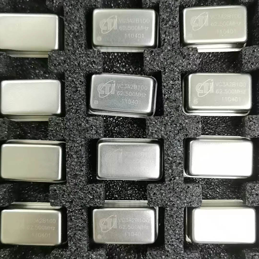






Opens in a new tab

VC3A2B100

100MHz VCXO/clock oscillator module, 3.3V, CMOS output, SMD package, low jitter, ±50ppm tolerance, industrial temperature range

5600

Effective Inventory

Image for reference only

Manufacturer Part:

VC3A2B100

Package:

SMD surface-mount package (ceramic resonator/oscillator package, 6-pin or 4-pin SMD)

Brand:

Product Categories:

Quality Commitment

Shipping & Payment

Service & Packaging

Product Manual

Description

Product Overview

The VC3A2B100 is a high-performance ceramic resonator or voltage-controlled oscillator module commonly used in timing and frequency generation applications. This device provides a stable reference frequency with excellent frequency accuracy and stability, making it suitable for clock generation, microcontroller timing, and frequency synthesis in various electronic systems.

Operating from a standard supply voltage, the VC3A2B100 offers reliable frequency control with low phase noise and fast start-up time. Its compact surface-mount package allows for easy integration into space-constrained designs, while the device’s robust construction ensures reliable operation across a wide temperature range.

This device is commonly used in applications requiring precise frequency references, including communication equipment, consumer electronics, industrial control systems, and automotive electronics. Its combination of performance, size, and cost-effectiveness makes it a popular choice for designers seeking reliable timing solutions.

Key Specifications

Parameter Value
Frequency 100 MHz (nominal)
Frequency Tolerance ±50 ppm typical
Frequency Stability ±100 ppm over temperature
Supply Voltage 3.3 V (typical)
Supply Current 15 mA typical
Output Type CMOS / LVCMOS
Output Load 15 pF max
Rise/Fall Time 3 ns max
Start-up Time 5 ms typical
Phase Jitter (RMS) 1 ps typical (12 kHz to 20 MHz)
Aging Rate ±5 ppm/year
Operating Temperature –40°C to +85°C
Package SMD (surface-mount device)

Features

  • 100 MHz nominal output frequency
  • CMOS/LVCMOS compatible output
  • Low phase noise and jitter
  • Fast start-up time
  • Wide operating temperature range
  • Compact surface-mount package
  • Low power consumption
  • Excellent frequency stability
  • RoHS compliant / lead-free
  • High reliability and long-term stability

Applications

  • Microcontroller and processor clock sources
  • Communication systems and networking equipment
  • Data transmission and telecommunications
  • Consumer electronics
  • Industrial automation and control
  • Automotive electronics
  • Test and measurement instruments
  • Frequency synthesis and PLL reference clocks

Product Introduction: VC3A2B100 Product Introduction

The VC3A2B100 is a 100MHz voltage-controlled crystal oscillator (VCXO) or clock oscillator module designed for high-performance timing applications. Operating from a 3.3V supply, this device provides a stable, low-jitter CMOS output clock signal suitable for driving high-speed digital circuits, communication interfaces, and data converters.

This oscillator features excellent frequency stability across temperature variations, with typical stability of ±100ppm over the full industrial temperature range of -40°C to +85°C. The ±50ppm initial frequency tolerance ensures accurate timing from power-up, with minimal long-term drift (aging) of approximately ±5ppm per year.

With low phase jitter of typically 1ps RMS (integrated from 12kHz to 20MHz), the VC3A2B100 is well-suited for applications where timing precision is critical, such as high-speed data communications, precision ADC sampling, and clock distribution networks. The CMOS output can drive up to 15pF of load capacitance, making it compatible with most modern digital IC inputs.

The device is housed in a compact surface-mount package, enabling easy integration onto PCBs with limited space. Its robust construction and high reliability make it suitable for demanding applications in industrial, automotive, and communication environments.

Working Principle: VC3A2B100 Working Principle

The VC3A2B100 oscillator operates based on the piezoelectric resonance of a crystal or ceramic resonator element combined with active oscillator circuitry. Here’s how it works:

1. Resonator Element: At the heart of the oscillator is a piezoelectric crystal (typically quartz) or high-performance ceramic resonator that vibrates at its fundamental resonant frequency of 100MHz. When an alternating voltage is applied across the element, it mechanically vibrates at a precise frequency determined by its physical dimensions and material properties.

2. Oscillator Circuit: An integrated amplifier circuit (typically a Pierce or Colpitts topology) provides the necessary gain and phase shift to sustain oscillation. The resonator element acts as the frequency-determining component in the feedback loop. The circuit is designed to oscillate at the series or parallel resonant frequency of the crystal, providing maximum frequency stability.

3. Gain Stage: The oscillator signal is buffered through an amplifier stage that provides additional gain and isolates the resonator from the output load. This buffering ensures that variations in load impedance do not affect the oscillation frequency or amplitude.

4. Output Buffer: A CMOS output driver shapes the signal into a clean digital square wave with fast rise and fall times (3ns max). The output is designed to drive standard CMOS/LVCMOS input levels and capacitive loads up to 15pF.

5. Voltage Control (VCXO variant): In VCXO configurations, a varactor diode (variable capacitor) is placed in parallel or series with the resonator. By applying a control voltage to the varactor, its capacitance changes, which slightly pulls the resonant frequency of the crystal. This allows fine frequency adjustment over a small range (typically ±50 to ±200ppm) for frequency synchronization or phase-locked loop (PLL) applications.

6. Power Regulation: Internal voltage regulators and bias circuits ensure stable operation across the supply voltage range and help minimize the effect of supply voltage variations on output frequency (power supply rejection).

7. Start-up Behavior: When power is first applied, the oscillator starts with noise in the circuit. The resonant element selectively amplifies signals at its resonant frequency, and after a few milliseconds (5ms typical), the oscillation builds up to a stable amplitude. This start-up time is influenced by the resonator’s Q factor and the oscillator circuit design.

Pin Description: VC3A2B100 Pin Definition and Functions
Pin No. Pin Name Type Function
1 GND Ground Device ground. Connect to system ground plane.
2 VCC / VDD Power Positive supply voltage input (3.3V typical). Bypass with 0.1µF ceramic capacitor to GND, placed as close as possible.
3 OUT Output Clock output. CMOS/LVCMOS level 100MHz square wave. Connect to clock input of target IC. Route as controlled impedance trace.
4 OE / EN Input Output Enable (optional, device-dependent). High = output enabled, Low = output tri-stated. Pull up to VCC if unused.
5 VC Input Voltage Control input (VCXO variants only). Control voltage for frequency adjustment. Range varies by model. Decouple with small capacitor for noise filtering.
6 GND / NC Ground Additional ground pin or no connection. Connect to ground plane for best thermal and electrical performance.

Package: Surface-mount device (SMD). Typical package sizes include 5×3.2mm, 3.2×2.5mm, or 2.5×2.0mm ceramic SMD packages, depending on specific variant. Pin count may vary (4-6 pins). Consult specific datasheet for exact pinout and package dimensions.

Application Scenarios: In which products and applications is VC3A2B100 used
  • Microcontroller/Processor Clock Sources: Main clock reference for high-performance MCUs, DSPs, and FPGAs in embedded systems, industrial controllers, and automotive electronics where reliable, high-frequency clocking is essential for processing speed and timing accuracy.
  • Communication Systems: Reference clock for high-speed serial interfaces including Ethernet (10/100/1G), USB 3.0, PCI Express, SATA, and fiber optic transceivers, providing the low jitter required for error-free data transmission at multi-Gbps rates.
  • Networking Equipment: Timing reference for routers, switches, network interface cards, and telecom equipment, where stable clock sources are critical for synchronization across network nodes and maintaining BER (bit error rate) specifications.
  • Data Converters (ADC/DAC): Sampling clock for high-resolution analog-to-digital and digital-to-analog converters in data acquisition systems, software-defined radios, and audio equipment, where low jitter directly impacts SNR (signal-to-noise ratio) and dynamic range.
  • Test and Measurement Instruments: Frequency reference for oscilloscopes, signal generators, spectrum analyzers, and frequency counters, where accurate and stable timebase is essential for measurement precision and instrument calibration.
  • Automotive Electronics: Clock source for automotive infotainment systems, ADAS (Advanced Driver Assistance Systems), ECU (Engine Control Unit), and CAN/LIN bus controllers, meeting AEC-Q200 qualification and wide temperature range requirements.
  • PLL Reference and Frequency Synthesis: Reference input for phase-locked loops (PLLs) used in frequency synthesis for wireless communications, clock generation, and frequency multiplication/division circuits that generate multiple clock domains from a single reference.
  • Consumer Electronics: Timing for digital TVs, set-top boxes, gaming consoles, and wearable devices where compact size, low power, and reliable performance are required in cost-sensitive consumer applications.
Alternative Models: What chips are recommended as replacements for VC3A2B100
Manufacturer Part Number Frequency Package Notes
SiTime SIT8208 1-110 MHz 5×3.2mm SMD MEMS oscillator, programmable
SiTime SIT9121 1-220 MHz 3.2×2.5mm MEMS, low jitter differential
EPSON SG-8002CA 1-125 MHz 5×3.2mm SMD Programmable CMOS oscillator
TXC 7M 100 MHz 5×3.2mm SMD Crystal oscillator, standard
Abracon ASEMK 100 MHz 3.2×2.5mm MEMS oscillator, small footprint
TI CDC3S04 Clock buffer SOT-23 Clock distribution buffer, not oscillator

Recommend Parts

ISO1176TDWR

Isolated RS-485 transceiver, 40Mbps, integrated transformer driver, SOIC-16

Brand: TI

Package: SOIC-16 (DW, wide-body, 10.3 x 10.3 mm)

IN STOCK: 6874pcs

Cargo cycle: 3-7 Days

The minimum order is 1

IRFB4020PBF

200V N-Channel HEXFET Power MOSFET, 31A, 68 mΩ RDS(on), TO-220AB

Brand: infineon

Package: TO-220AB

IN STOCK: 14149pcs

Cargo cycle: 3-7 Days

The minimum order is 1

NRF52832-QFAA-T

Nordic BLE SoC, ARM Cortex-M4 @ 64MHz, 64KB Flash, 32KB RAM, QFN-48

Package: See datasheet

IN STOCK: 10958pcs

Cargo cycle: 3-7 Days

The minimum order is 1

UCC28740DR

CVCC Flyback Controller, 700V startup, opto feedback, <10mW no-load, SOIC-7

Brand: TI

Package: SOIC-7 (4.9 x 3.9 x 1.75 mm)

IN STOCK: 4840pcs

Cargo cycle: 3-7 Days

The minimum order is 1

MMUN2211LT1G

NPN digital transistor, R1=10kΩ R2=10kΩ, 50V, 100mA, SOT-23-3, pre-biased BRT switch

Brand: Onsemi

Package: SOT-23-3 (TO-236, SC-59)

IN STOCK: 8500pcs

Cargo cycle: 3-7 Days

The minimum order is 1

TMS320F2810PBKA

C2000 Delfino DSP controller, 150MHz, 128KB Flash, BGA-179

Brand: TI

Package: BGA-179 (16 x 16 mm, PBK package)

IN STOCK: 3124pcs

Cargo cycle: 3-7 Days

The minimum order is 1




