






Opens in a new tab

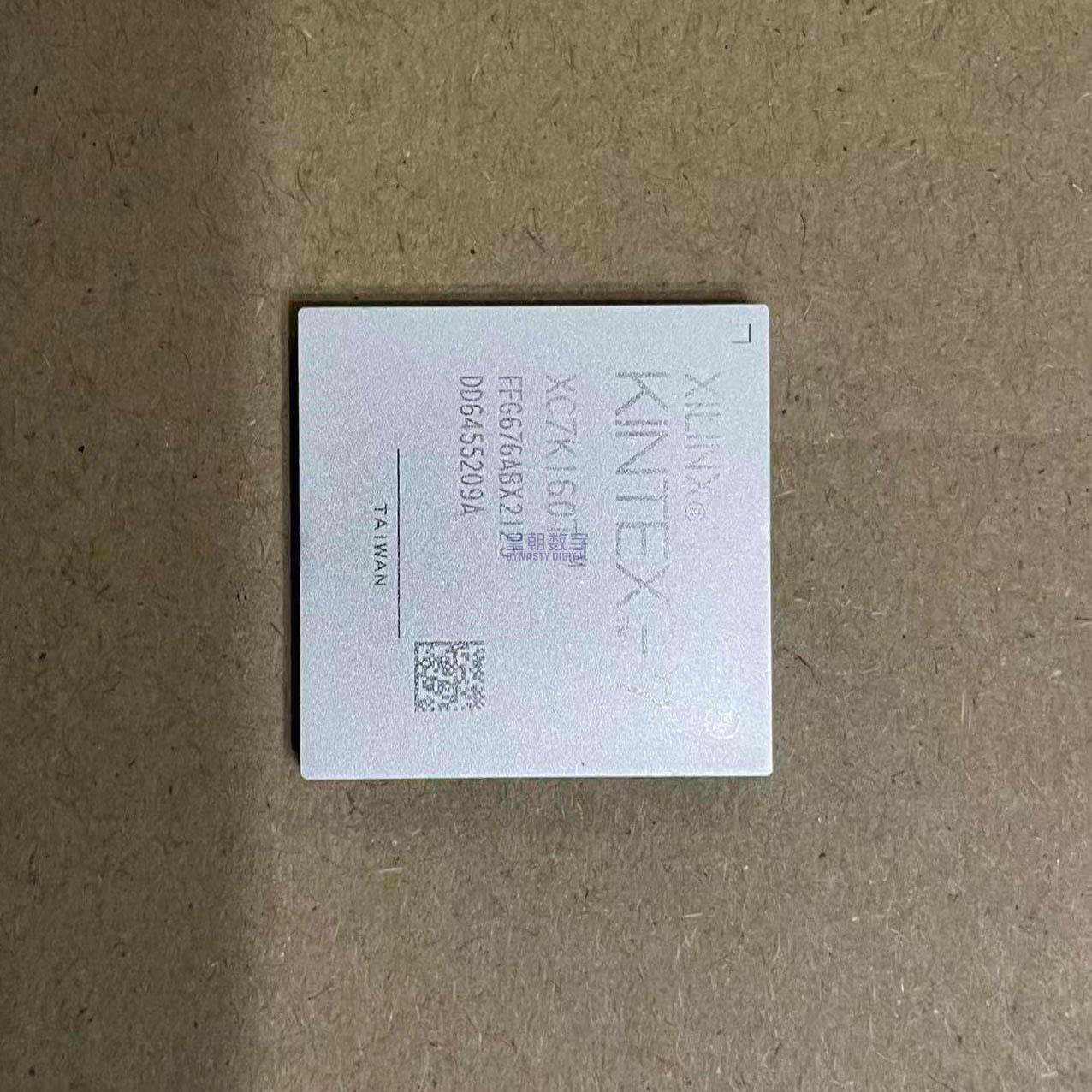
XC7K160T-2FFG676I

Kintex-7 FPGA, 162K logic cells, 600 DSP, 11.6MB BRAM, 16 GTX 12.5Gbps, PCIe Gen2 x8, DDR3 1866Mbps, FCBGA-676 27x27mm, -2 industrial, 28nm HKMG, AMD Xilinx

320

Effective Inventory

Image for reference only

Manufacturer Part:

XC7K160T-2FFG676I

Package:

FFG676 (676-ball flip-chip fine-pitch BGA, 27x27mm body, 1.0mm ball pitch, flip-chip die attachment, 8 I/O banks, industrial grade)

Brand:

Quality Commitment

Shipping & Payment

Service & Packaging

Product Manual

Description

Product Overview

The XC7K160T-2FFG676I is a Kintex-7 FPGA from Xilinx (AMD), featuring 162,240 logic cells in a 676-ball Fine-pitch Flip-chip BGA package. As the entry-level member of the Kintex-7 family, this device delivers exceptional price-performance with high-speed serial connectivity, substantial DSP capacity, and advanced memory interfaces at a mid-range cost point.

Built on 28 nm high-k metal gate (HKMG) process technology, the XC7K160T integrates 25,350 CLB slices with 202,800 flip-flops, 600 DSP48E1 slices for high-performance signal processing, and 324 block RAMs totaling 11,664 Kb of embedded memory. Ten clock management tiles (CMTs), each containing an MMCM and a PLL, provide extensive clock synthesis capabilities. The device includes up to 16 GTX transceivers operating at up to 12.5 Gb/s (data rate dependent on speed grade), an integrated PCIe Gen2 x8 endpoint block, and a dedicated memory interface controller supporting DDR3 at up to 1,866 Mb/s.

The FFG676 package measures 27 x 27 mm with 1.0 mm flip-chip ball pitch, providing up to 500 user I/O pins across 8 high-performance (HP) banks supporting 3.3V-tolerant I/O standards. The -2 speed grade with industrial temperature range (-40 degC to +100 degC junction) delivers excellent performance for demanding communications, signal processing, and industrial applications. Kintex-7 offers the best price-performance-per-watt in the Xilinx 7-series portfolio.

Key Specifications

Parameter Value
Logic Cells 162,240
CLB Slices 25,350 (202,800 flip-flops)
Distributed RAM (max) ~1,980 Kb
Block RAM (36 Kb each) 324 blocks = 11,664 Kb total
DSP48E1 Slices 600 (25×18 multiplier + 48-bit accumulator)
CMT (MMCM + PLL) 10 (10 MMCMs + 10 PLLs)
GTX Transceivers 16 (up to 12.5 Gb/s each)
PCIe Endpoint Block 1 (Gen2 x8, 5.0 Gb/s per lane)
Memory Interface Controller 1 (DDR3/DDR3L up to 1,866 Mb/s)
Ethernet MACs 2 (1G/2.5G with GMII/RGMII/SGMII)
I/O Banks 8 HP banks (high-performance)
Max User I/Os (FFG676) Up to 500 (3.3V tolerant HR + HP mixed)
Max LVDS Data Rate 1,600 Mb/s (differential)
Core Voltage 1.0 V
Auxiliary Voltage 1.8 V
MGT AVCC 1.0 V
Speed Grade -2 (industrial I-grade)
Max DSP Clock ~450 MHz (-2 speed grade)
Configuration SPI x1/x2/x4/x8, BPI x16, JTAG, SelectMAP, Quad SPI
Package FFG676 / FCBGA-676 (27×27 mm, 1.0 mm pitch, flip-chip)
Junction Temperature -40 degC to +100 degC (industrial)

Features

  • Kintex-7 family: best price-performance-per-watt mid-range FPGA
  • 162,240 logic cells with 6-input LUT architecture
  • 600 DSP48E1 slices for high-performance DSP
  • 11,664 Kb block RAM + ~1,980 Kb distributed RAM
  • 10 CMTs with MMCMs and PLLs for comprehensive clocking
  • 16 GTX transceivers: up to 12.5 Gb/s per channel
  • Integrated PCI Express Gen2 x8 endpoint block
  • DDR3/DDR3L memory interface: up to 1,866 Mb/s
  • Dual 1G/2.5G Ethernet MACs
  • Up to 500 user I/O pins across 8 banks
  • 50+ I/O standards: LVCMOS, LVDS, LVPECL, HSTL, SSTL
  • 1.6 Gb/s LVDS differential data rate
  • AES-256 bitstream encryption, HMAC authentication
  • Device DNA unique identifier for anti-cloning
  • MultiBoot / Fallback configuration support
  • Advanced power management: suspend / hibernate
  • 28 nm HKMG process technology
  • MicroBlaze 32-bit soft processor support
  • Vivado Design Suite and ISE compatible
  • Industrial temperature: -40 degC to +100 degC TJ
  • FFG676 flip-chip BGA package, lead-free

Applications

  • 4G LTE / 5G wireless infrastructure
  • Wired networking and high-end routers
  • Software-defined radio and radar processing
  • High-end medical imaging (CT, MRI, ultrasound)
  • Broadcast video infrastructure and production switching
  • Aerospace and defense systems
  • High-speed test and measurement equipment
  • Data center FPGA acceleration
Product Introduction: XC7K160T-2FFG676I Product Introduction

The XC7K160T-2FFG676I is the entry-level member of Xilinx’s (AMD) Kintex-7 FPGA family, offering 162,240 logic cells, 600 DSP slices, and 16 high-speed GTX transceivers in a 676-ball flip-chip fine-pitch BGA package. The Kintex-7 family is renowned for delivering the industry’s best price-performance-per-watt ratio in the mid-range FPGA segment, bridging the gap between cost-optimized Artix-7 and high-end Virtex-7 families.

Built on TSMC’s 28nm high-k metal gate (HKMG) process, the Kintex-7 architecture provides a substantial step up from Artix-7 in terms of serial transceiver count, DSP density, and memory interface performance. The XC7K160T includes 25,350 CLB slices with 202,800 flip-flops, enabling complex logic designs with extensive pipelining. Approximately half of the slices are SLICEMs supporting distributed RAM and shift register functionality.

DSP performance is a key Kintex-7 strength: 600 DSP48E1 slices, each with a 25×18-bit multiplier, 48-bit accumulator, and pre-adder. Operating at frequencies up to 450MHz in the -2 speed grade, these DSP slices deliver enormous signal processing throughput for applications like wireless baseband processing, radar beamforming, and high-end video processing.

High-speed serial connectivity is provided by 16 GTX transceivers capable of data rates up to 12.5 Gb/s per channel. These support protocols including PCI Express (via dedicated Gen2 x8 endpoint block), 10 Gigabit Ethernet, CPRI, SRIO, SATA, Aurora, Interlaken, and more. The integrated PCIe block supports up to x8 lane width at Gen2 speeds, enabling high-bandwidth host CPU connectivity.

A hardened memory interface controller supports DDR3 and DDR3L at data rates up to 1,866 Mb/s, providing high memory bandwidth for data-intensive applications. Dual tri-mode Ethernet MACs (1G/2.5G) further reduce system cost and logic utilization.

The FFG676 flip-chip package provides superior thermal performance and signal integrity compared to wire-bond packages. With 500 user I/O pins across 8 banks and industrial temperature rating (TJ -40 to +100 degC), this device is well-suited for the most demanding communications, industrial, and aerospace applications.

Working Principle: XC7K160T-2FFG676I Working Principle

The Kintex-7 XC7K160T is a high-performance 28nm FPGA implementing custom digital logic through configurable logic blocks, advanced routing, high-speed serial transceivers, and hardened IP blocks. Key architecture:

1. Configurable Logic Blocks (CLBs): 25,350 CLB slices in a regular array. Each slice contains four 6-input LUTs and eight flip-flops. SLICEM slices (~50%) support distributed RAM (64-bit per LUT), SRL32 shift registers, and wide multiplexer functions. A hierarchical routing structure provides fast local connections and long-distance routes with optimized delay and power consumption.

2. Block RAM (BRAM): 324 dedicated 36Kb block RAMs arranged in columns. Each supports true dual-port operation, simple dual-port, or single-port mode with byte write enables. Can be split into two 18Kb blocks. Built-in FIFO controllers simplify FIFO implementation. Total BRAM: 11,664Kb – sufficient for large frame buffers, packet stores, and DSP coefficient tables.

3. DSP48E1 Slices: 600 DSP slices in two columns for high-throughput signal processing. Each contains a 25×18-bit signed multiplier, 48-bit accumulator, pre-adder, pattern detector, and optional pipeline registers. Supports operations at ~450 MHz in -2 speed grade. Cascading enables wider arithmetic. Ideal for FIR/IIR filters, FFT, complex arithmetic, matrix operations, and finite state machine optimization.

4. Clock Management: Ten CMT blocks, each with one MMCM (Mixed-Mode Clock Manager) and one PLL. MMCMs provide very precise fractional-N frequency synthesis, phase shifting, deskew, and duty cycle correction with extremely low jitter. PLLs offer additional clock multiplication/division. Global clock networks and regional clocks distribute signals with minimal skew across the device.

5. GTX Transceivers: 16 high-speed serial transceivers organized in quads (4 per quad). Each supports line rates from ~500 Mb/s up to 12.5 Gb/s. Includes PCS (Physical Coding Sublayer) with 8b/10b encoding/decoding and PMA (Physical Media Attachment) with CDR, TX pre-emphasis, and RX equalization. Supports a wide range of protocols: PCIe, 10G Ethernet, CPRI (up to 9.8 Gbps), SRIO, Aurora, SATA, Interlaken, and custom protocols.

6. PCI Express Block: Dedicated PCIe endpoint block supporting Gen2 (5.0 Gb/s) up to x8 lane width. Includes physical, data link, and transaction layers in hardened IP, significantly reducing FPGA logic utilization and design complexity. Supports both endpoint and root port configurations.

7. Memory Interface Generator (MIG): Hardened memory controller with advanced PHY supporting DDR3/DDR3L at up to 1,866 Mb/s data rates. Includes calibration, leveling, and training capabilities for robust operation across voltage and temperature variations. Delivers high bandwidth for data buffering and processing applications.

8. Configuration: Bitstream loads from SPI Flash, parallel NOR (BPI), or JTAG. Advanced security features include AES-256 bitstream encryption and HMAC-SHA-256 authentication. Device DNA provides a unique identifier per device for anti-cloning and license management. MultiBoot supports multiple bitstream images with fallback.

Pin Description: XC7K160T-2FFG676I Pin Definition and Functions
Pin Group Description
VCCINT Core logic supply: 1.0 V. Many VCCINT balls distributed across the package for power integrity. All must be connected with appropriate decoupling capacitors.
VCCAUX Auxiliary supply: 1.8 V. Powers CMTs, configuration logic, and auxiliary circuits.
VMGTAVCC GTX transceiver analog supply: 1.0 V. Powers GTX transceiver analog circuits. Requires careful filtering and isolation for optimal jitter performance.
VMGTAVTT GTX transceiver termination supply: 1.2 V. Powers output drivers and termination circuits of GTX transceivers.
VCCBANK0-7 I/O bank supply voltages. Eight independent banks. Each bank can operate at different Vcco voltages depending on the I/O standards used. HP banks support up to 2.0V, HR banks up to 3.3V.
GND Ground reference. Extensive ground balls throughout the package for signal integrity, power distribution, and thermal dissipation.
User I/O Pins Up to 500 general-purpose I/O pins. Configurable for single-ended (LVCMOS, LVTTL, HSTL, SSTL, etc.) or differential (LVDS, LVPECL, differential HSTL/SSTL) standards. 8 banks total.
MRCC/SRCC Pins Clock-capable I/O pins with dedicated routing to CMTs. Multi-region and single-region clock capable inputs for external clock sources.
GTX Pins (MGT) GTX transceiver differential pairs: RXP/N (receive) and TXP/N (transmit) for each of 16 channels. Connect to high-speed serial data channels. Organized in banks of 4 (quad).
GTX Reference Clocks MGTREFCLK P/N pairs – dedicated differential reference clock inputs for GTX transceiver quads. Low-jitter clock sources required for optimal performance.
Configuration Pins CCLK, D0-D7 (parallel data), DIN, DOUT, CSI_B, RDWR_B, INIT_B, DONE, PROGRAM_B, M0/M1/M2 (mode selection), FCS_B, FOE_B, FWE_B (BPI mode).
JTAG Pins TCK, TMS, TDI, TDO. IEEE 1149.1 boundary scan and JTAG device configuration. JTAG chain can be shared with other devices.
DONE Pin Open-drain output indicating successful configuration completion. Typically pulled up to VCCAUX.

Package: FFG676 – Flip-chip Fine-pitch Ball Grid Array, 676 balls. Body: 27mm x 27mm. Ball pitch: 1.0mm. Ball array: approximately 26×26 grid. Flip-chip die attachment for better thermal dissipation and electrical performance. 8 I/O banks. Industrial temperature grade (TJ: -40 degC to +100 degC). RoHS compliant, lead-free.

Application Scenarios: In which products and applications is XC7K160T-2FFG676I used
  • 4G LTE and 5G Wireless Infrastructure: Baseband processing in LTE/5G base stations, including channel coding/decoding, FFT/IFFT, and digital pre-distortion (DPD) for power amplifier linearization. 600 DSP slices + 16 GTX transceivers (supporting CPRI up to 9.8 Gbps) provide the necessary signal processing and fronthaul connectivity for multi-standard radio systems.
  • Wired Networking and High-End Routers: Packet processing, traffic management, and high-speed interface bridging in core/edge routers, carrier Ethernet switches, and optical transport network (OTN) equipment. 16 GTX transceivers handle 10GbE/OTU2/4 interfaces, while the large logic capacity implements deep packet inspection and QoS functions.
  • Software-Defined Radio and Radar Processing: High-performance SDR platforms, radar signal processing, and electronic warfare systems where the combination of 600 DSP slices, high-speed transceivers, and large on-chip memory enables wideband signal processing, beamforming, and real-time spectral analysis.
  • Medical Imaging (CT, MRI, Ultrasound): High-end medical imaging systems including CT reconstruction, MRI gradient control, and 3D ultrasound beamforming requiring massive DSP computational power, high-speed serial data links to ADC/DAC arrays, and large memory buffers for raw data storage and processing pipelines.
  • Broadcast Video Infrastructure: 4K/8K video processing, production switchers, multi-viewers, format converters, and broadcast routing equipment where Kintex-7’s DSP resources handle video scaling, deinterlacing, and compression, while GTX transceivers provide 12G-SDI and HDMI 2.0/2.1 interfaces.
  • Aerospace and Defense: Radar processing, electronic countermeasures, secure communications, and satellite systems where the industrial temperature rating, advanced security features (AES-256 + HMAC), and long lifecycle support meet stringent defense requirements. Flip-chip packaging provides excellent thermal and mechanical reliability.
  • High-Speed Test and Measurement: High-performance oscilloscopes, signal analyzers, protocol test equipment, and ATE systems requiring very high-speed serial capture, real-time DSP analysis, deep memory, and extensive I/O for probe channels and interface ports.
  • Data Center FPGA Acceleration: Computational acceleration cards for data centers, including machine learning inference, financial trading, database acceleration, and network security, where the PCIe Gen2 x8 interface provides high host bandwidth and 16 GTX transceivers support network/storage connectivity.
Alternative Models: What chips are recommended as replacements for XC7K160T-2FFG676I
Manufacturer Part Number Logic Cells DSP BRAM Transceivers Package Notes
Xilinx/AMD XC7K325T-2FFG676I 326,080 840 16,020 Kb 16 GTX FCBGA-676 Larger, same package
Xilinx/AMD XC7K160T-2FBG676C 162,240 600 11,664 Kb 16 GTX FCBGA-676 Commercial temperature grade
Xilinx/AMD XC7A200T-2FBG676I 215,360 740 13,140 Kb 16 GTX FBGA-676 Artix-7, lower cost
Intel/Altera EP4SGX110HF35C4 110,500 LE 548 M9K 6,120 Kb 24 GX BGA-1152 Stratix IV GX, larger pkg
Intel/Altera 10AX016E3F29I2SG 155,000 LE 480 M10K 5,320 Kb 12 GX BGA-672 Arria 10 GX, 20nm
Lattice LFE5UM5G-85F-8FCBG756I 84 K LUT 156 DSP 3,378 Kb 6 SERDES csfBGA-756 ECP5-5G, lower cost

Recommend Parts

ISO1176TDWR

Isolated RS-485 transceiver, 40Mbps, integrated transformer driver, SOIC-16

Brand: TI

Package: SOIC-16 (DW, wide-body, 10.3 x 10.3 mm)

IN STOCK: 6874pcs

Cargo cycle: 3-7 Days

The minimum order is 1

IRFB4020PBF

200V N-Channel HEXFET Power MOSFET, 31A, 68 mΩ RDS(on), TO-220AB

Brand: infineon

Package: TO-220AB

IN STOCK: 14149pcs

Cargo cycle: 3-7 Days

The minimum order is 1

NRF52832-QFAA-T

Nordic BLE SoC, ARM Cortex-M4 @ 64MHz, 64KB Flash, 32KB RAM, QFN-48

Package: See datasheet

IN STOCK: 10958pcs

Cargo cycle: 3-7 Days

The minimum order is 1

UCC28740DR

CVCC Flyback Controller, 700V startup, opto feedback, <10mW no-load, SOIC-7

Brand: TI

Package: SOIC-7 (4.9 x 3.9 x 1.75 mm)

IN STOCK: 4840pcs

Cargo cycle: 3-7 Days

The minimum order is 1

MMUN2211LT1G

NPN digital transistor, R1=10kΩ R2=10kΩ, 50V, 100mA, SOT-23-3, pre-biased BRT switch

Brand: Onsemi

Package: SOT-23-3 (TO-236, SC-59)

IN STOCK: 8500pcs

Cargo cycle: 3-7 Days

The minimum order is 1

TMS320F2810PBKA

C2000 Delfino DSP controller, 150MHz, 128KB Flash, BGA-179

Brand: TI

Package: BGA-179 (16 x 16 mm, PBK package)

IN STOCK: 3124pcs

Cargo cycle: 3-7 Days

The minimum order is 1





