






Opens in a new tab

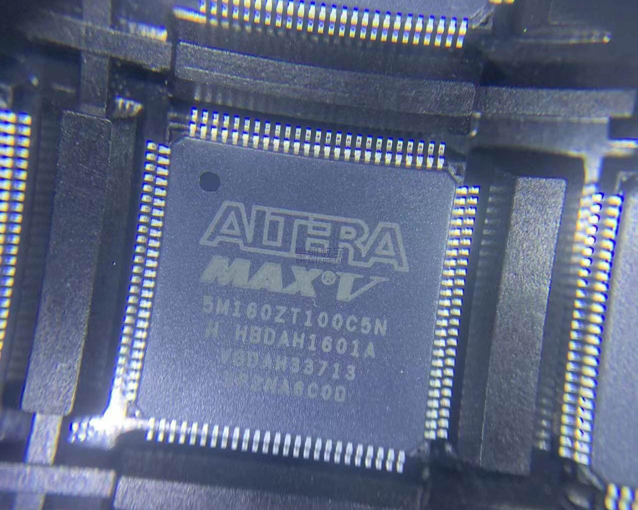
5M160ZT100C5N

Intel MAX V CPLD, 160 logic elements, 128 macrocells, 79 I/O pins, 8Kbit UFM, 7.5ns delay, 1.8V core, 100-TQFP package, flash-based non-volatile instant-on operation.

4250

Effective Inventory

Image for reference only

Manufacturer Part:

5M160ZT100C5N

Package:

100-TQFP (14mm x 14mm)

Brand:

Quality Commitment

Shipping & Payment

Service & Packaging

Product Manual

Description

Product Overview

The 5M160ZT100C5N is a MAX V series CPLD (Complex Programmable Logic Device) from Intel (formerly Altera), offering 160 logic elements (equivalent to 128 macrocells) in a 100-pin TQFP package. As part of Intel’s low-cost, low-power MAX V family built on 180nm process technology, this device combines non-volatile flash-based configuration with instant-on operation and low standby power consumption. With 79 user I/O pins, 8Kbit of user flash memory, and a 7.5ns pin-to-pin propagation delay at speed grade -5, the 5M160ZT100C5N provides flexible logic integration for cost-sensitive applications including industrial control, consumer electronics, and communication systems. The device features MultiVolt I/O support for 1.2V, 1.5V, 1.8V, 2.5V, and 3.3V standards, along with built-in JTAG programming and boundary-scan capabilities.

Key Specifications

Parameter Value
Logic Elements (LE) 160
Equivalent Macrocells 128
Speed Grade -5 (7.5ns pin-to-pin delay)
User I/O Pins 79
I/O Banks 2
User Flash Memory (UFM) 8 Kbit
Internal Supply Voltage 1.71 V to 1.89 V (1.8V nominal)
MultiVolt I/O Standards 1.2V, 1.5V, 1.8V, 2.5V, 3.3V
JTAG Boundary-Scan Yes (IEEE 1149.1)
In-System Programmability Yes (via JTAG)
Internal Oscillator Yes (user-accessible)
Schmitt Trigger Inputs Yes
Programmable Slew Rate Yes
Programmable Pull-Up Resistors Yes
Open-Drain Outputs Yes
Bus-Hold Feature Yes
Operating Temperature 0°C to +85°C (TJ)
Package 100-Pin TQFP (14mm x 14mm)
Process Technology 180 nm Flash/CMOS

Features

  • Non-volatile flash-based CPLD with instant-on operation
  • 160 logic elements (128 equivalent macrocells) in 100-TQFP package
  • Fast pin-to-pin propagation delay: 7.5ns at -5 speed grade
  • 79 user I/O pins with MultiVolt I/O support (1.2V to 3.3V)
  • Integrated 8Kbit user flash memory (UFM) for non-volatile data storage
  • Low standby power consumption for battery-operated applications
  • JTAG in-system programmability (ISP) for field updates
  • Built-in user-accessible internal oscillator
  • Fast power-on reset for system initialization
  • LVTTL/LVCMOS I/O standards with emulated LVDS outputs
  • Programmable output slew rate for EMI control
  • Programmable pull-up resistors and bus-hold on I/O pins
  • Supported by Intel Quartus Prime design software
  • RoHS compliant and halogen-free packaging

Applications

  • Industrial automation and control systems
  • Consumer electronics – TVs, cameras, home appliances
  • Communication systems and interface bridging
  • Power supply management and sequencing
  • Boot sequencing and configuration control
  • Legacy hardware replacement and glue logic
  • Test and measurement equipment
  • Automotive electronics (non-safety)
  • Data storage and peripheral interfaces
  • Embedded system co-processors and state machines

Product Introduction: 5M160ZT100C5N Product Introduction

The 5M160ZT100C5N is a member of Intel’s MAX V family of complex programmable logic devices (CPLDs), designed to provide a cost-effective, low-power solution for digital logic integration and system control applications. Built on 180nm flash CMOS process technology, the MAX V series combines the non-volatility and instant-on characteristics of traditional CPLDs with the low cost and high density associated with FPGA architectures. With 160 logic elements (equivalent to approximately 128 macrocells), this device provides sufficient logic capacity for a wide range of general-purpose logic functions, state machines, and interface bridging applications. The 100-pin TQFP package offers 79 user I/O pins organized into two I/O banks, each supporting MultiVolt I/O operation at 1.2V, 1.5V, 1.8V, 2.5V, or 3.3V LVCMOS/LVTTL standards. This multi-voltage capability enables seamless interfacing between different voltage domains without requiring external level translators. The integrated 8Kbit user flash memory (UFM) provides non-volatile storage for serial numbers, calibration data, configuration parameters, or small lookup tables, eliminating the need for external serial EEPROM in many designs. The device also features an internal oscillator that can be used as a clock source for simple state machines and timing functions, further reducing external component count. The JTAG interface supports both in-system programming (ISP) and boundary-scan testing per IEEE 1149.1, enabling field updates and manufacturing test capabilities. The -5 speed grade provides a pin-to-pin propagation delay of 7.5ns, delivering fast combinational logic performance. The 5M160ZT100C5N operates from a 1.8V core supply (1.71V to 1.89V range) with an operating junction temperature range of 0°C to 85°C for commercial applications. Designed using Intel’s Quartus Prime design software, which is available as a free download, the MAX V series offers an accessible development platform for both prototype and production designs. The devices are particularly well-suited for replacing discrete logic components, reducing board space and bill of materials cost in consumer electronics, industrial controls, communication systems, and automotive applications.

Working Principle: 5M160ZT100C5N Working Principle

A CPLD (Complex Programmable Logic Device) is a semiconductor device that can be programmed to implement custom digital logic functions. The 5M160ZT100C5N uses a flash-based architecture where the configuration data is stored in non-volatile flash memory cells within the device, providing instant-on operation – the device is operational immediately after power-up without requiring configuration from an external memory device like most FPGAs. The core architecture consists of an array of logic elements (LEs) interconnected through a programmable routing matrix. Each logic element contains a look-up table (LUT) for implementing combinational logic functions, a flip-flop for sequential logic, and dedicated carry-chain logic for arithmetic operations. The LUTs can be configured to implement any Boolean function of their inputs. The programmable interconnect matrix provides routing resources to connect logic elements together and to the I/O pins, with the specific connections determined by the user’s design programmed into the configuration flash. The MultiVolt I/O architecture allows each I/O bank to be powered by a separate supply voltage, enabling the device to directly interface with components operating at different voltage levels without external level-shifting circuitry. I/O features including programmable slew rate control, pull-up resistors, bus-hold circuits, open-drain capability, and Schmitt trigger inputs provide flexibility for various interface requirements. The user flash memory (UFM) is an independent non-volatile storage block that can be accessed through the device’s logic fabric or via the JTAG interface, providing 8Kbits of storage for application data. The internal oscillator provides a free-running clock signal that can be used by user logic for simple timing functions, eliminating the need for an external crystal or oscillator in cost-sensitive applications. Configuration is performed through the JTAG interface using Intel’s Quartus Prime software, which compiles the user’s hardware description language (HDL) design into a configuration bitstream that is then programmed into the device’s internal flash memory.

Pin Description: 5M160ZT100C5N Pin Definition and Functions
Pin Group Description
I/O Pins (79 pins) General-purpose user I/O pins organized into 2 banks (Bank 1 and Bank 2); each bank has its own VCCIO supply supporting 1.2V, 1.5V, 1.8V, 2.5V, or 3.3V; configurable as input, output, or bi-directional with various I/O standards
VCCINT (1.8V) Core logic power supply pins; 1.71V to 1.89V operating range; multiple VCCINT pins distributed around the package for power distribution
VCCIO (Bank 1 & 2) I/O bank power supply pins; each bank has independent VCCIO for MultiVolt operation; voltage determines the I/O standard supported by that bank
GND Ground reference pins; multiple GND pins distributed for optimal power distribution and signal integrity
TCK JTAG test clock input – clock signal for JTAG boundary scan and in-system programming
TMS JTAG test mode select – controls the state of the JTAG TAP controller
TDI JTAG test data input – serial data input for JTAG operations and programming
TDO JTAG test data output – serial data output from JTAG operations
CONFIG_IO / nSTATUS Configuration status and I/O configuration select pins; indicate device configuration state
Application Scenarios: In which products and applications is 5M160ZT100C5N used
  • Industrial automation control logic and PLC I/O expansion
  • Consumer electronics – TVs, set-top boxes, cameras, home appliances
  • Communication system interface bridging and protocol conversion
  • Power supply sequencing, monitoring, and management functions
  • System boot sequence control and configuration management
  • Replacement of 74-series discrete logic ICs to reduce BOM cost and board space
  • Automotive body electronics and infotainment systems (non-safety critical)
  • Test and measurement equipment front-end logic
  • Data storage interface controllers and peripheral bridges
  • Embedded system state machines, event sequencers, and custom logic accelerators
Alternative Models: What chips are recommended as replacements for 5M160ZT100C5N
Model Manufacturer Key Difference
XC95144XL Xilinx / AMD 144 macrocells CPLD, 5ns delay, competing flash-based CPLD
5M80ZT100C5N Intel Same package, smaller – 80 LE / 64 macrocells, lower cost
5M240ZT100C5N Intel Same package, larger – 240 LE / 192 macrocells, higher density
LC4128V-75TN100C Lattice 128 macrocells ispMACH 4000 series CPLD, TQFP-100
XC2C128-7VQG100C Xilinx / AMD CoolRunner-II 128 macrocells, low power CPLD, QFP-100

Recommend Parts

ISO1176TDWR

Isolated RS-485 transceiver, 40Mbps, integrated transformer driver, SOIC-16

Brand: TI

Package: SOIC-16 (DW, wide-body, 10.3 x 10.3 mm)

IN STOCK: 6874pcs

Cargo cycle: 3-7 Days

The minimum order is 1

IRFB4020PBF

200V N-Channel HEXFET Power MOSFET, 31A, 68 mΩ RDS(on), TO-220AB

Brand: infineon

Package: TO-220AB

IN STOCK: 14149pcs

Cargo cycle: 3-7 Days

The minimum order is 1

NRF52832-QFAA-T

Nordic BLE SoC, ARM Cortex-M4 @ 64MHz, 64KB Flash, 32KB RAM, QFN-48

Package: See datasheet

IN STOCK: 10958pcs

Cargo cycle: 3-7 Days

The minimum order is 1

UCC28740DR

CVCC Flyback Controller, 700V startup, opto feedback, <10mW no-load, SOIC-7

Brand: TI

Package: SOIC-7 (4.9 x 3.9 x 1.75 mm)

IN STOCK: 4840pcs

Cargo cycle: 3-7 Days

The minimum order is 1

MMUN2211LT1G

NPN digital transistor, R1=10kΩ R2=10kΩ, 50V, 100mA, SOT-23-3, pre-biased BRT switch

Brand: Onsemi

Package: SOT-23-3 (TO-236, SC-59)

IN STOCK: 8500pcs

Cargo cycle: 3-7 Days

The minimum order is 1

TMS320F2810PBKA

C2000 Delfino DSP controller, 150MHz, 128KB Flash, BGA-179

Brand: TI

Package: BGA-179 (16 x 16 mm, PBK package)

IN STOCK: 3124pcs

Cargo cycle: 3-7 Days

The minimum order is 1




