
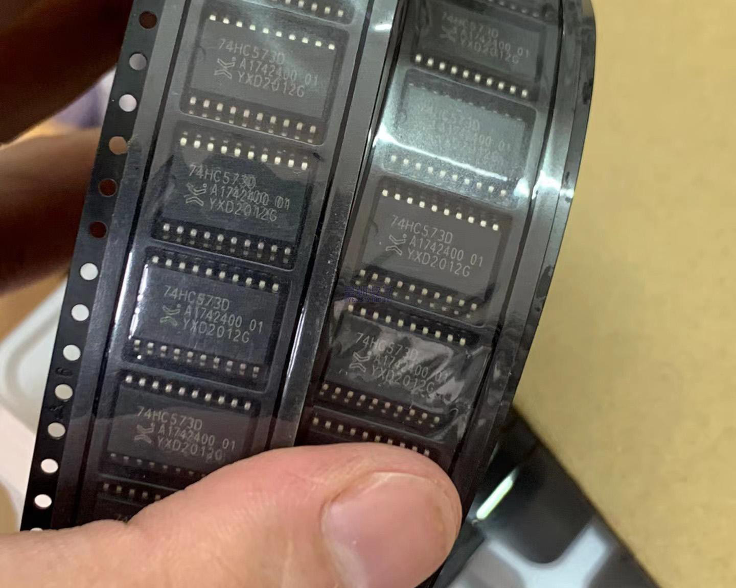






Opens in a new tab

74HC573D

Octal D-type transparent latch with 3-state outputs, 8-bit, 2.0-6.0V supply, ±7.8mA output, 14ns delay, SO20 package, flow-through pinout, 74HC CMOS logic family.

12860

Effective Inventory

Image for reference only

Manufacturer Part:

74HC573D

Package:

SO20 / SOIC-20

Brand:

Product Categories:

Quality Commitment

Shipping & Payment

Service & Packaging

Product Manual

Description

Product Overview

The 74HC573D is a high-speed CMOS octal D-type transparent latch with 3-state outputs, manufactured by Nexperia. This 8-bit latch features separate D-type inputs for each latch and 3-state true outputs ideal for bus-oriented applications. Controlled by a common latch enable (LE) input and output enable (OE) input, the device operates in transparent mode when LE is HIGH, with outputs following the D inputs directly. When LE goes LOW, the data present at the inputs is latched and held. A HIGH on OE places all eight outputs in a high-impedance OFF-state without affecting the stored latch data. Operating from a 2.0V to 6.0V supply range and packaged in an SO20 surface-mount package, the 74HC573D is specified over the -40°C to +125°C industrial temperature range and offers flow-through pin organization that simplifies microprocessor and bus interface designs.

Key Specifications

Parameter Value
Logic Family 74HC (High-Speed CMOS)
Function Octal D-Type Transparent Latch, 3-State Output
Number of Bits 8 (Octal)
Output Type 3-State, Non-Inverting (True Output)
Supply Voltage Range (VCC) 2.0 V to 6.0 V
Input Logic Levels CMOS (74HC573)
Output Drive Current ±7.8 mA (max at 4.5V VCC)
Propagation Delay D→Q 14 ns (typ) @ VCC=4.5V
Propagation Delay LE→Q 15 ns (typ) @ VCC=4.5V
Setup Time (ts, min) 14 ns @ VCC=4.5V
Hold Time (th, min) 5 ns @ VCC=4.5V
Minimum LE Pulse Width 16 ns @ VCC=4.5V
Quiescent Supply Current (ICC) 4.0 µA (max) @ 25°C
ESD Protection (HBM) >2000 V (JESD22-A114F Class 2)
Latch-Up Performance >100 mA per JESD 78 Class II Level B
Operating Temperature Range -40°C to +125°C
Package SO20 / SOIC-20 (SOT163-1)
Compliance JEDEC JESD8C, JESD7A; RoHS compliant

Features

  • 8-bit D-type transparent latch with 3-state outputs for bus interface
  • Wide supply voltage range: 2.0V to 6.0V
  • CMOS low power dissipation with high noise immunity
  • Flow-through pin organization for easy microprocessor interface
  • Common latch enable (LE) and output enable (OE) controls
  • Non-inverting 3-state outputs drive bus lines directly
  • Balanced propagation delays with tPLH ≈ tPHL
  • Input clamp diodes for overvoltage protection and level shifting
  • Latch-up performance exceeds 100mA per JESD 78 Class II Level B
  • ESD protection exceeds 2000V HBM and 1000V CDM
  • Functionally identical to 74HC373 but with different pin arrangement
  • Available in multiple packages: SO20, TSSOP20, SSOP20, DIP20, DHVQFN20
  • Specified from -40°C to +125°C for industrial applications

Applications

  • Microprocessor and microcomputer data bus latches
  • Input/output port expansion for embedded systems
  • Address latching in memory decoding circuits
  • Bus-oriented data storage and transfer
  • Data acquisition and control systems
  • Industrial automation and process control
  • Consumer electronics and communication equipment
  • General-purpose digital logic storage

Product Introduction: 74HC573D Product Introduction

The 74HC573D is an octal D-type transparent latch from Nexperia’s 74HC high-speed CMOS logic family, designed for general-purpose data storage and bus interface applications. This 8-bit latch features eight individual D-type data inputs and eight 3-state non-inverting outputs, all controlled by common latch enable (LE) and output enable (OE) signals. When the latch enable (LE) input is HIGH, the latch operates in transparent mode where the Q outputs directly follow the D inputs – any change on a D input immediately appears on the corresponding Q output. When LE transitions from HIGH to LOW, the data present at the D inputs at that moment is captured and held in the latch, regardless of subsequent changes on the inputs. The output enable (OE) controls the 3-state output buffers independently of the latch state. When OE is LOW, the latched data is presented at the outputs. When OE is HIGH, all outputs enter a high-impedance state, disconnecting from the bus but preserving the stored latch data. This allows multiple devices to share a common data bus without conflict. The flow-through pin arrangement (inputs on one side, outputs on the other) simplifies PCB layout, particularly for microprocessor bus interface designs. Operating from a 2.0V to 6.0V supply range with CMOS input levels, the 74HC573D offers typical propagation delays of 14ns (D to Q) at 4.5V supply. The device features input clamp diodes, latch-up immunity exceeding 100mA, and ESD protection greater than 2000V HBM. Packaged in the standard SO20 (SOT163-1) surface-mount package with 1.27mm pitch, the device is specified over the extended industrial temperature range of -40°C to +125°C and is fully compliant with JEDEC standards JESD8C and JESD7A. The 74HC573D is functionally identical to the 74HC373 but features a different pin configuration that is often preferred for bus-oriented designs.

Working Principle: 74HC573D Working Principle

The 74HC573D is a CMOS-based transparent latch, meaning that when the latch enable (LE) signal is HIGH, the output Q follows the input D (the latch is ‘transparent’). When LE goes LOW, the value of D at that moment is captured and held at the output, even if D subsequently changes. Each of the eight latch channels consists of a master latch stage that accepts the D input data when LE is HIGH, and a slave/output stage that drives the Q output. In transparent mode (LE=HIGH), the master latch is open and continuously passes the D input through to the slave stage, so Q=D. When LE goes LOW, the master latch closes and holds the last value, isolating the output from further input changes. The 3-state output buffer is controlled by the output enable (OE) signal. When OE is LOW, the output buffer is enabled and drives the latched data onto the output pin. When OE is HIGH, the output buffer is disabled and enters a high-impedance state where the pin is effectively floating, allowing bus sharing with other devices. Importantly, the OE signal does not affect the internal latch state – data remains latched and stored even when OE is HIGH. The CMOS implementation provides very low static power consumption, with quiescent current in the microamp range. The output stage uses complementary PMOS/NMOS transistors for rail-to-rail output swing and balanced sourcing/sinking capability. Setup and hold times define the timing requirements around the LE falling edge: the D input must be stable for at least the setup time before LE falls, and must remain stable for at least the hold time after LE falls, to ensure reliable latching. The device is designed to be robust with input protection diodes, latch-up immunity, and extensive ESD protection.

Pin Description: 74HC573D Pin Definition and Functions
Pin No. Name Description
1 OE Output Enable (active LOW); when HIGH, all Q outputs are high-impedance; does not affect latch state
2 D0 Data input for latch bit 0 (LSB)
3 D1 Data input for latch bit 1
4 D2 Data input for latch bit 2
5 D3 Data input for latch bit 3
6 D4 Data input for latch bit 4
7 D5 Data input for latch bit 5
8 D6 Data input for latch bit 6
9 D7 Data input for latch bit 7 (MSB)
10 GND Ground (0V supply)
11 LE Latch Enable (active HIGH); HIGH = transparent mode (Q follows D); LOW = latch and hold
12 Q7 3-state latch output for bit 7 (MSB)
13 Q6 3-state latch output for bit 6
14 Q5 3-state latch output for bit 5
15 Q4 3-state latch output for bit 4
16 Q3 3-state latch output for bit 3
17 Q2 3-state latch output for bit 2
18 Q1 3-state latch output for bit 1
19 Q0 3-state latch output for bit 0 (LSB)
20 VCC Positive supply voltage, 2.0V to 6.0V
Application Scenarios: In which products and applications is 74HC573D used
  • Microprocessor and microcomputer data bus interface latches
  • I/O port expansion for microcontroller and embedded systems
  • Address latching in memory and peripheral decoding circuits
  • Bus-oriented data storage and parallel data transfer
  • Data acquisition systems holding sampled data
  • Industrial control and automation systems
  • Consumer electronics: TVs, set-top boxes, audio equipment
  • General-purpose parallel data storage and register applications
Alternative Models: What chips are recommended as replacements for 74HC573D
Model Manufacturer Key Difference
74HCT573D Nexperia Same function, TTL-level inputs, 4.5-5.5V supply only
74HC573PW Nexperia Same function, TSSOP-20 package, smaller board footprint
74HC373D Nexperia Functionally identical, different pinout (74LS373 style)
74HC563D Nexperia Inverting output version, same package and timing
SN74HC573 Texas Instruments Equivalent octal latch, 74HC family, TI manufacturer

Recommend Parts

ISO1176TDWR

Isolated RS-485 transceiver, 40Mbps, integrated transformer driver, SOIC-16

Brand: TI

Package: SOIC-16 (DW, wide-body, 10.3 x 10.3 mm)

IN STOCK: 6874pcs

Cargo cycle: 3-7 Days

The minimum order is 1

IRFB4020PBF

200V N-Channel HEXFET Power MOSFET, 31A, 68 mΩ RDS(on), TO-220AB

Brand: infineon

Package: TO-220AB

IN STOCK: 14149pcs

Cargo cycle: 3-7 Days

The minimum order is 1

NRF52832-QFAA-T

Nordic BLE SoC, ARM Cortex-M4 @ 64MHz, 64KB Flash, 32KB RAM, QFN-48

Package: See datasheet

IN STOCK: 10958pcs

Cargo cycle: 3-7 Days

The minimum order is 1

UCC28740DR

CVCC Flyback Controller, 700V startup, opto feedback, <10mW no-load, SOIC-7

Brand: TI

Package: SOIC-7 (4.9 x 3.9 x 1.75 mm)

IN STOCK: 4840pcs

Cargo cycle: 3-7 Days

The minimum order is 1

MMUN2211LT1G

NPN digital transistor, R1=10kΩ R2=10kΩ, 50V, 100mA, SOT-23-3, pre-biased BRT switch

Brand: Onsemi

Package: SOT-23-3 (TO-236, SC-59)

IN STOCK: 8500pcs

Cargo cycle: 3-7 Days

The minimum order is 1

TMS320F2810PBKA

C2000 Delfino DSP controller, 150MHz, 128KB Flash, BGA-179

Brand: TI

Package: BGA-179 (16 x 16 mm, PBK package)

IN STOCK: 3124pcs

Cargo cycle: 3-7 Days

The minimum order is 1




