






Opens in a new tab

Home » Integrated Circuits ICs » AD8244BRMZ

AD8244BRMZ

Quad JFET-input unity-gain buffer, 2pA max bias current, 10TΩ input impedance, 13nV/√Hz noise, 3MHz bandwidth, 3-36V single supply, rail-to-rail output, 10-MSOP, ADI.

5240

Effective Inventory

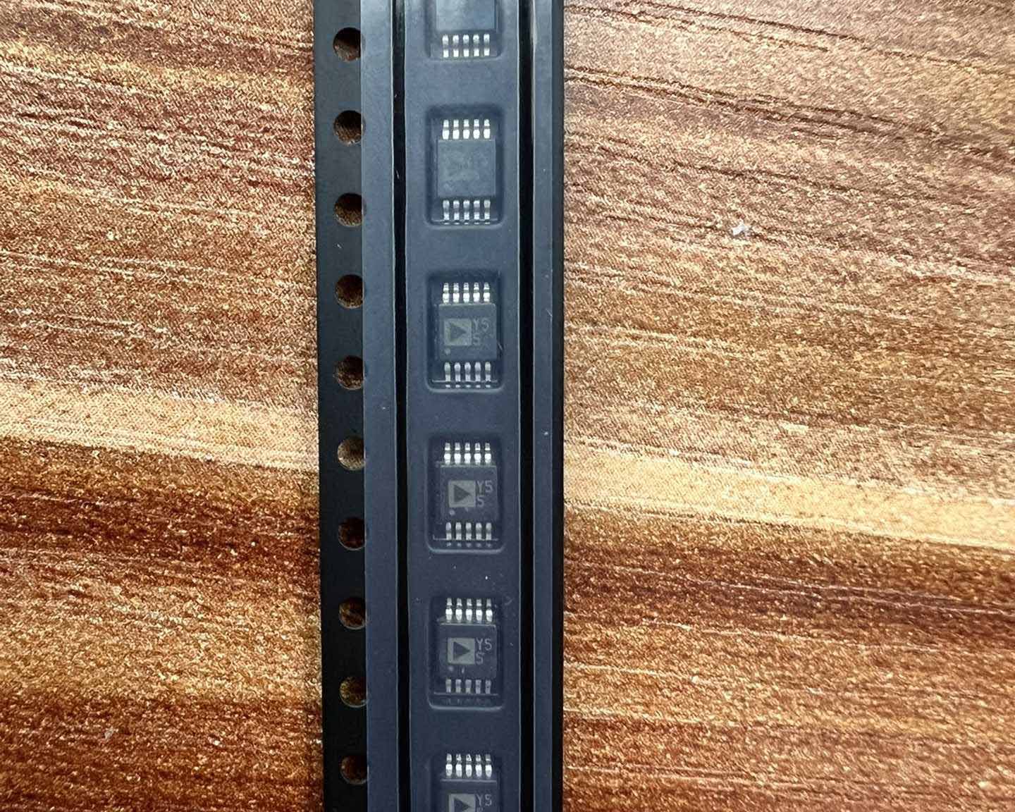
Image for reference only

Manufacturer Part:

AD8244BRMZ

Package:

10-Lead MSOP

Product Categories:

Quality Commitment

Shipping & Payment

Service & Packaging

Product Manual

Description

Product Overview

The AD8244BRMZ is a precision, low-power, FET-input quad unity-gain buffer from Analog Devices, designed to isolate very high source impedances from the rest of the signal chain. Featuring JFET inputs with 2 pA maximum bias current at 25°C, near-zero current noise (0.8 fA/√Hz), and 10 TΩ input impedance, the AD8244 introduces almost no error even when driving sources with megaohm-level impedances. The B-grade AD8244BRMZ achieves high DC precision with 350 µV maximum offset voltage and 3 µV/°C maximum offset drift over temperature. Each channel draws only 250 µA maximum supply current while delivering 3 MHz bandwidth and rail-to-rail output performance. A unique pinout physically separates high-impedance inputs from low-impedance supplies and other buffer outputs, simplifying PCB guard ring layout for high-impedance circuits. Packaged in a compact 10-lead MSOP, the AD8244BRMZ is specified over the industrial temperature range of -40°C to +85°C and is ideal for biopotential electrodes, medical instrumentation, high-impedance sensor conditioning, filters, and photodiode amplifiers.

Key Specifications

Parameter Value
Number of Channels 4 (Quad)
Amplifier Type JFET-Input Unity-Gain Buffer
Closed-Loop Gain 1 V/V (unity-gain, internally connected)
Input Bias Current (25°C) 2 pA (max), 0.5 pA (typ)
Input Bias Current (85°C) 50 pA (max)
Input Offset Voltage (B-grade, 25°C) 350 µV (max)
Offset Drift (B-grade, -40°C to +85°C) 3 µV/°C (max)
Input Impedance 10 TΩ || 4 pF
Voltage Noise Density (1 kHz) 13 nV/√Hz (typ)
Voltage Noise (0.1 Hz to 10 Hz) 0.4 µV p-p (typ)
Current Noise Density (1 kHz) 0.8 fA/√Hz (typ)
Gain Bandwidth Product 3 MHz (typ)
Slew Rate 0.8 V/µs (typ)
0.01% Settling Time 8 µs (typ) for 2.8V step
Supply Voltage Range (Single) 3 V to 36 V
Supply Voltage Range (Dual) ±1.5 V to ±18 V
Supply Current per Amplifier 250 µA (max), 210 µA (typ)
Input Voltage Range 0 V to V+ – 4 V (single supply, extends to ground)
Output Voltage Swing (10kΩ load to GND) 0.025 V to 4.9 V (5V supply, typ)
Output Short-Circuit Current 8 mA (typ)
Capacitive Load Drive 200 pF
Channel-to-Channel Offset Matching 500 µV (typ)
Channel-to-Channel Gain Matching 0.08% (typ)
Package 10-Lead MSOP
Operating Temperature Range -40°C to +85°C

Features

  • Quad JFET-input unity-gain buffer with extremely low bias current: 2 pA max
  • Ultra-high input impedance: 10 TΩ for high-impedance source isolation
  • Low voltage noise: 13 nV/√Hz at 1 kHz; 0.4 µV p-p 0.1-10 Hz
  • Near-zero current noise: 0.8 fA/√Hz at 1 kHz
  • High DC precision: 350 µV max offset (B-grade), 3 µV/°C max drift
  • Low power consumption: 250 µA per amplifier maximum supply current
  • Wide supply range: 3V to 36V single supply, ±1.5V to ±18V dual supply
  • 3 MHz bandwidth and 0.8 V/µs slew rate
  • Rail-to-rail output with single-supply operation
  • Input range extends to ground (negative supply rail)
  • Unique pinout separates high-impedance inputs from supply pins for easy guarding
  • Compact 10-lead MSOP package (traditional quad op-amp needs 14 pins)
  • Excellent channel-to-channel matching for differential applications
  • Unity-gain stable with capacitive load drive capability
  • 4 channels can be paralleled to reduce voltage noise by half
  • Industrial temperature range: -40°C to +85°C

Applications

  • Biopotential electrodes and medical instrumentation (ECG, EEG, EMG)
  • High-impedance sensor signal conditioning
  • Photodiode preamplifiers and frontends
  • Active filter input buffering
  • Data acquisition input isolation and buffering
  • Piezoelectric sensor amplifiers
  • pH electrodes and electrochemical sensor interfaces
  • DAC output buffering and load isolation
  • Low-noise precision signal chains
  • Portable and battery-powered instruments

Product Introduction: AD8244BRMZ Product Introduction

The AD8244BRMZ is a precision four-channel JFET-input unity-gain buffer from Analog Devices, specifically designed to provide ultra-high input impedance buffering for high-impedance signal sources. Unlike traditional operational amplifiers configured as buffers, the AD8244 is purpose-built as a unity-gain buffer, eliminating the need for external feedback components and optimizing the design for the buffer function. The device features N-channel JFET input transistors that provide extremely low input bias current of 2 pA maximum at 25°C, near-zero current noise of 0.8 fA/√Hz, and an exceptional input impedance of 10 TΩ. This makes the AD8244 ideal for interfacing with high-impedance sources such as photodiodes, piezoelectric sensors, biopotential electrodes, and high-value resistive sensors where even tiny input currents would introduce significant errors. The B-grade AD8244BRMZ offers high DC accuracy with a maximum input offset voltage of 350 µV at 25°C and a maximum offset temperature coefficient of 3 µV/°C over the full operating temperature range. The rail-to-rail output stage swings to within 25 mV of the supply rails with a 10 kΩ load, maximizing the output dynamic range, especially in low-voltage single-supply systems. A unique and important design feature of the AD8244 is its innovative pinout. Unlike traditional quad op-amp packages where power supply pins are positioned next to high-impedance input pins (creating leakage paths that can swamp the fA-level bias currents), the AD8244’s pinout physically separates the high-impedance inputs from the low-impedance supplies and outputs of other buffers. This dramatically simplifies PCB guard ring design, allowing compact board layouts while maintaining the ultra-high impedance performance. The 10-lead MSOP package is significantly smaller than a conventional 14-pin quad op-amp package, providing higher channel density. The AD8244 operates from a wide supply range of 3V to 36V single supply (or ±1.5V to ±18V dual supply), making it compatible with a broad range of system voltages. With only 250 µA supply current per channel, it is well-suited for low-power and battery-powered applications. The 3 MHz bandwidth and 0.8 V/µs slew rate provide adequate speed for many precision signal conditioning applications. An interesting application technique enabled by the quad configuration is paralleling all four buffers to reduce the voltage noise by half (from 13 nV/√Hz to approximately 6.5 nV/√Hz), since uncorrelated noise sources add in an RMS fashion. The AD8244BRMZ is specified over the industrial temperature range of -40°C to +85°C and is ideal for medical instrumentation, high-impedance sensor interfaces, photodiode amplification, active filters, and general-purpose high-impedance buffering applications.

Working Principle: AD8244BRMZ Working Principle

The AD8244 is a purpose-built unity-gain buffer amplifier that uses JFET input transistors to achieve ultra-high input impedance and very low input bias current. Each buffer channel consists of a JFET differential input stage followed by additional gain stages and a rail-to-rail output stage, all configured for unity gain with internal feedback. The JFET (junction field-effect transistor) input stage is what gives the device its extremely high input impedance and low bias current characteristics. JFETs operate by controlling current through a channel using an electric field, and the gate terminal is essentially insulated by a reverse-biased PN junction, resulting in gate currents that are measured in picoamps or femtoamps rather than microamps as in BJT input amplifiers. This makes JFET inputs ideal for buffering very high impedance signal sources. Because the AD8244 is configured as a unity-gain buffer (voltage follower), the output is connected directly back to the inverting input internally, creating a feedback loop that forces the output voltage to precisely follow the input voltage. The unity-gain configuration provides the widest possible bandwidth, fastest settling, and best stability for a given amplifier. The rail-to-rail output stage uses complementary transistors that can swing very close to both supply rails, maximizing the output voltage range. The input common-mode range extends down to the negative supply (ground in single-supply operation), which is particularly useful for AC-coupled or ground-referenced signals. A key innovation of the AD8244 is the physical layout that separates high-impedance input pins from power supply and output pins. In conventional op-amp packages, the proximity of supply pins to input pins creates parasitic leakage paths through surface contamination and PCB material. For JFET-input amplifiers with pA-level bias currents, even minute leakage (nanoamps or even hundreds of picoamps) can severely degrade performance. By placing the high-impedance inputs on one side of the package and the low-impedance supply/output pins on the other, the AD8244 allows the PCB designer to easily implement a guard ring around the input pins that follows the input voltage, preventing leakage currents from reaching the sensitive input node. The channel-to-channel matching of the AD8244 is also carefully controlled, enabling the four channels to be used in differential signal chains with minimal error. Additionally, paralleling multiple buffer outputs (with small balancing resistors) can reduce the total voltage noise by a factor equal to the square root of the number of paralleled channels.

Pin Description: AD8244BRMZ Pin Definition and Functions
Pin No. Name Description
1 +INA Non-inverting input of buffer A – high-impedance JFET input; connect to signal source
2 OUTA Output of buffer A – buffered output follows +INA voltage
3 +INB Non-inverting input of buffer B – high-impedance JFET input; connect to signal source
4 OUTB Output of buffer B – buffered output follows +INB voltage
5 VS- Negative supply voltage – ground in single-supply operation; connect to lowest potential
6 +INC Non-inverting input of buffer C – high-impedance JFET input; connect to signal source
7 OUTC Output of buffer C – buffered output follows +INC voltage
8 +IND Non-inverting input of buffer D – high-impedance JFET input; connect to signal source
9 OUTD Output of buffer D – buffered output follows +IND voltage
10 VS+ Positive supply voltage – 3V to 36V single supply; decouple to VS- with capacitors

Note: The unique pinout separates high-impedance input pins from supply and output pins, simplifying PCB guard ring design for high-impedance applications. Input pins (1, 3, 6, 8) are interleaved with output pins (2, 4, 7, 9) on one side, while supply pins (5, 10) are on opposite sides and far from input pins.

Application Scenarios: In which products and applications is AD8244BRMZ used
  • Biopotential electrode buffering for ECG, EEG, EMG, and other medical instrumentation
  • High-impedance sensor signal conditioning: piezoelectric, piezoresistive, MEMS sensors
  • Photodiode preamplifiers and optical receiver frontends
  • Active filter input stages and high-impedance filter networks
  • pH electrodes and electrochemical/ion-selective electrode interfaces
  • DAC output buffering for driving resistive or capacitive loads
  • Data acquisition system input isolation and impedance matching
  • Low-noise precision signal chains where high input Z is critical
  • Portable and battery-powered test and measurement instruments
  • Charge amplifier input stages for piezoelectric sensors
  • Instrumentation amplifier input protection and buffering
Alternative Models: What chips are recommended as replacements for AD8244BRMZ
Model Manufacturer Key Difference
AD8244ARMZ Analog Devices A-grade version, 600µV max offset voltage, same package
AD8628 Analog Devices Single JFET-input op-amp with auto-zero, lower noise, different topology
LMP7704 Texas Instruments Quad precision low-input-bias CMOS op-amp, alternative
OPA4140 Texas Instruments Quad JFET-input op-amp, 18MHz, higher speed, SOIC-14
ADA4625-1 Analog Devices Single 36V precision JFET op-amp, lower bias current

Recommend Parts

ISO1176TDWR

Isolated RS-485 transceiver, 40Mbps, integrated transformer driver, SOIC-16

Brand: TI

Package: SOIC-16 (DW, wide-body, 10.3 x 10.3 mm)

IN STOCK: 6874pcs

Cargo cycle: 3-7 Days

The minimum order is 1

IRFB4020PBF

200V N-Channel HEXFET Power MOSFET, 31A, 68 mΩ RDS(on), TO-220AB

Brand: infineon

Package: TO-220AB

IN STOCK: 14149pcs

Cargo cycle: 3-7 Days

The minimum order is 1

NRF52832-QFAA-T

Nordic BLE SoC, ARM Cortex-M4 @ 64MHz, 64KB Flash, 32KB RAM, QFN-48

Package: See datasheet

IN STOCK: 10958pcs

Cargo cycle: 3-7 Days

The minimum order is 1

UCC28740DR

CVCC Flyback Controller, 700V startup, opto feedback, <10mW no-load, SOIC-7

Brand: TI

Package: SOIC-7 (4.9 x 3.9 x 1.75 mm)

IN STOCK: 4840pcs

Cargo cycle: 3-7 Days

The minimum order is 1

MMUN2211LT1G

NPN digital transistor, R1=10kΩ R2=10kΩ, 50V, 100mA, SOT-23-3, pre-biased BRT switch

Brand: Onsemi

Package: SOT-23-3 (TO-236, SC-59)

IN STOCK: 8500pcs

Cargo cycle: 3-7 Days

The minimum order is 1

TMS320F2810PBKA

C2000 Delfino DSP controller, 150MHz, 128KB Flash, BGA-179

Brand: TI

Package: BGA-179 (16 x 16 mm, PBK package)

IN STOCK: 3124pcs

Cargo cycle: 3-7 Days

The minimum order is 1




