






Opens in a new tab

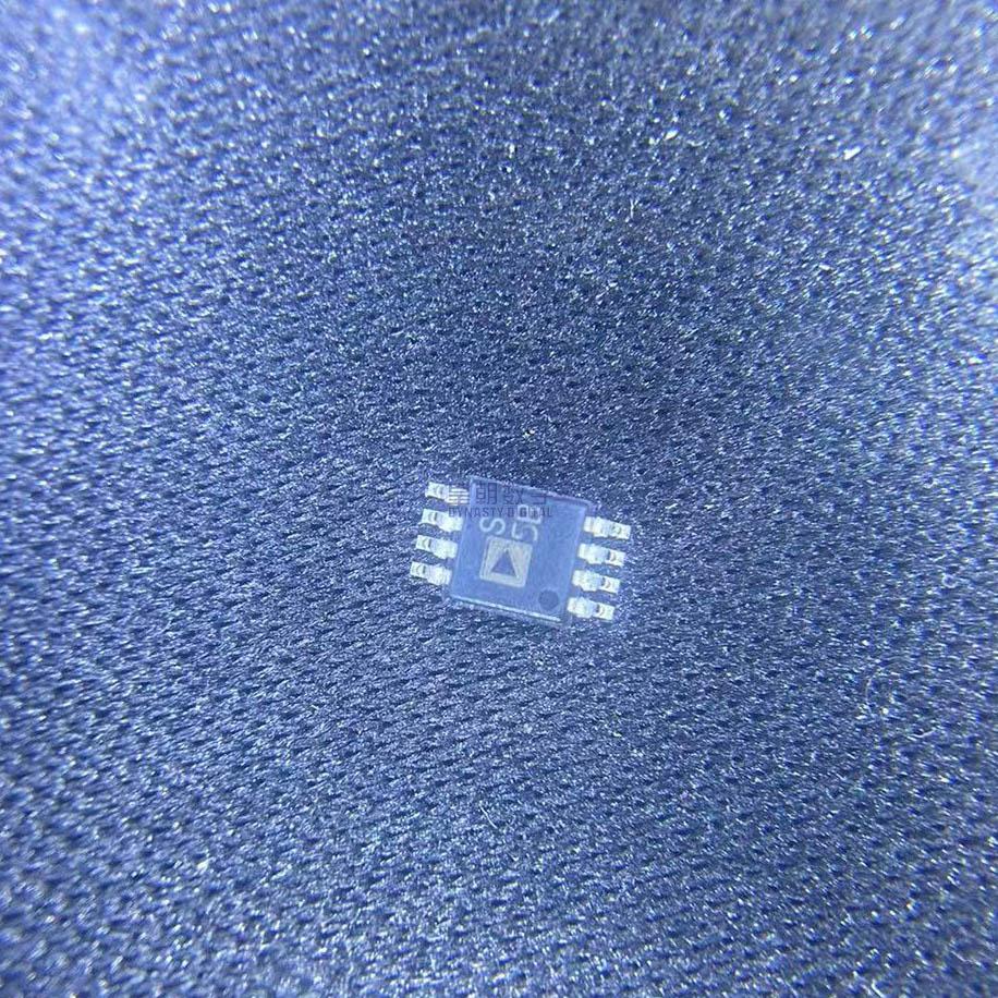
ADG719BRMZ

CMOS SPDT analog switch, 1.8-5.5V single supply, 4ohm RON max, 200MHz bandwidth, 7ns tON, break-before-make, uW power, 8-MSOP, ADI ADG7xx family.

12500

Effective Inventory

Image for reference only

Manufacturer Part:

ADG719BRMZ

Package:

8-Lead MSOP

Quality Commitment

Shipping & Payment

Service & Packaging

Product Manual

Description

Product Overview

The ADG719BRMZ is a monolithic CMOS single-pole double-throw (SPDT) switch from Analog Devices, designed on a submicron CMOS process for low power consumption, high switching speed, low on-resistance, and low leakage currents. Operating from a single 1.8V to 5.5V supply, the device is ideal for battery-powered instruments and interfacing with modern low-voltage DACs and ADCs. The ADG719 features break-before-make switching action, preventing momentary short circuits when switching between channels. On the 5V supply, the switch achieves a maximum on-resistance of 4 ohms with 0.75 ohm typical flatness across the signal range, and delivers over 200 MHz of -3dB bandwidth. The CMOS architecture ensures ultralow power consumption of less than 0.01 microwatts typical. The ADG719BRMZ is the B-grade industrial temperature version (-40C to +125C) in an 8-lead MSOP package with RoHS-compliant matte tin finish.

Key Specifications

Parameter Conditions Min Typ Max Unit
Switch Configuration SPDT (2:1 Mux) 1 circuit, double-throw —
Supply Voltage Range Single supply 1.8 — 5.5 V
Analog Signal Range 0 V to VDD (rail-to-rail) V
On-Resistance (RON) VDD=5V, IS=-10mA, 25C — 2.5 4 Ω
On-Resistance (RON) VDD=3V, IS=-10mA, 25C — 6 10 Ω
RON Flatness VDD=5V — 0.75 1.2 Ω
Source Off Leakage VDD=5.5V, 25C — ±0.01 ±0.25 nA
Channel On Leakage 25C — ±0.01 ±0.25 nA
Turn-On Time (tON) RL=300Ω, CL=35pF — 7 12 ns
Turn-Off Time (tOFF) RL=300Ω, CL=35pF — 3 6 ns
Break-Before-Make Delay — 1 8 — ns
-3dB Bandwidth RL=50Ω, CL=5pF — 200 — MHz
Off Isolation f=10MHz — -67 — dB
Channel-to-Channel Crosstalk f=10MHz — -62 — dB
Supply Current (IDD) 25C — 0.001 1.0 μA
Input Logic Levels TTL/CMOS compatible VIH=2.0V min, VIL=0.8V max —
Charge Injection — — 3 — pC
Package 8-Lead MSOP (RM-8) —
Operating Temperature B grade -40 — +125 degrees C
MSL Rating MSL1 (unlimited floor life) —

Features

  • Single supply operation: 1.8 V to 5.5 V
  • Low on-resistance: 4 ohms maximum at 5V supply
  • Low on-resistance flatness: 0.75 ohms typical
  • Wide -3dB bandwidth: > 200 MHz
  • Rail-to-rail analog signal range
  • Fast switching: tON=12ns max, tOFF=6ns max
  • Break-before-make switching action
  • Ultralow power consumption: < 0.01 µW typical
  • Low leakage currents: ±0.25 nA typical off-leakage
  • TTL/CMOS compatible digital inputs
  • Low charge injection: 3 pC typical
  • Excellent channel isolation: -67 dB off-isolation at 10 MHz
  • Available in 6-lead SOT-23 and 8-lead MSOP packages
  • Industrial temperature range: -40C to +125C (B grade)
  • Automotive applications supported
  • Enhanced product available for defense/aerospace (ADG719-EP)
  • RoHS compliant matte tin finish (Z suffix)
  • MSL1 moisture sensitivity rating

Applications

  • Sample-and-hold systems and analog data acquisition
  • Audio signal routing and switching
  • Video signal switching and routing
  • Communication systems and RF signal paths
  • Battery-powered portable instruments
  • Data acquisition front-end multiplexing
  • ADC input channel selection
  • DAC output routing and calibration switching
  • Industrial process control and automation
  • Test and measurement equipment
Product Introduction: ADG719BRMZ Product Introduction

The ADG719BRMZ is a high-performance single-pole double-throw (SPDT) analog switch from Analog Devices, fabricated on an advanced submicron CMOS process that delivers an excellent combination of low on-resistance, high bandwidth, fast switching speed, and ultralow power consumption. As a member of the ADG7xx family of low-voltage CMOS switches, the ADG719 is designed for single-supply operation from 1.8V to 5.5V, making it well-suited for battery-powered portable instruments as well as modern low-voltage signal chain designs using 3.3V or 1.8V supplies. The switch conducts equally well in both directions when on and supports rail-to-rail analog signals, meaning the input signal can range from 0V all the way to VDD without degradation of on-resistance performance. The break-before-make switching ensures that when switching between the two channels, the previously selected channel turns off before the new channel turns on, preventing momentary shorts that could cause glitches or damage to upstream circuitry. With -3dB bandwidth exceeding 200 MHz, the ADG719 is capable of switching high-frequency analog signals including RF, video, and fast data signals. The CMOS construction provides several key advantages: extremely low power consumption (less than 1 microwatt), low leakage currents at the nanoamp level, and TTL/CMOS compatible digital inputs that interface directly with standard logic families. The ADG719BRMZ specifically is the B-grade industrial temperature version, specified over the full -40C to +125C temperature range and packaged in an 8-lead MSOP (mini small-outline package) with RoHS-compliant matte tin lead finish (indicated by the Z suffix). For higher reliability requirements, an enhanced product version (ADG719-EP) is available with AQEC qualification and controlled manufacturing baseline for defense and aerospace applications.

Working Principle: ADG719BRMZ Working Principle

The ADG719BRMZ is a CMOS analog switch that uses complementary MOS transistors (both NMOS and PMOS) connected in parallel as the switching element between the source and drain terminals. When the switch is turned on by applying the appropriate logic level to the control input, both the NMOS and PMOS transistors conduct, creating a low-resistance path between the source and drain terminals. The parallel NMOS/PMOS architecture is what enables rail-to-rail operation: at low signal voltages near ground, the PMOS transistor provides most of the conduction; at high signal voltages near VDD, the NMOS transistor dominates; and in the middle of the range, both transistors contribute. This ensures that the on-resistance remains relatively flat across the entire input signal range, which is why the on-resistance flatness specification (0.75 ohm typical at 5V) is so low. When the switch is turned off, both transistors are cut off, leaving only the leakage current of the reverse-biased PN junctions, which is at the nanoamp level. The break-before-make timing ensures that during a switching transition, there is a brief period (minimum 1 ns, typical 8 ns) when both channels are off before the new channel turns on. This prevents both channels from being simultaneously on, which would create a momentary short between the two source terminals. The digital control input is compatible with both TTL and CMOS logic levels, and the input current is minimal. Because the switch is constructed from CMOS transistors, it draws virtually no quiescent current from the supply when in a static state, resulting in the ultralow power consumption characteristic of CMOS switches.

Pin Description: ADG719BRMZ Pin Definition and Functions
Pin No. Name Description
1 D Drain terminal (common terminal of the SPDT switch). Can be used as input or output depending on signal direction.
2 S1 Source 1 terminal (first throw position). Connected to D when switch selects S1 position.
3 GND Ground reference pin. 0V reference for the device.
4 VDD Positive power supply pin. Connect to 1.8V to 5.5V supply. Bypass with 0.1 uF capacitor to GND.
5 NC No internal connection. Not used in MSOP package.
6 IN Digital switch control input. Logic high selects S1; logic low selects S2.
7 NC No internal connection. Not used in MSOP package.
8 S2 Source 2 terminal (second throw position). Connected to D when switch selects S2 position.
Application Scenarios: In which products and applications is ADG719BRMZ used
  • Analog input multiplexing for data acquisition systems
  • Sample-and-hold circuit input switching
  • Audio signal routing in mixers, amplifiers, and audio equipment
  • Video switching and routing in video distribution and display systems
  • RF signal path switching in communication equipment
  • Battery-powered portable test and measurement instruments
  • ADC input channel selection and front-end signal conditioning
  • DAC output switching and calibration path routing
  • Industrial process control analog signal routing
  • Communication systems signal path configuration
Alternative Models: What chips are recommended as replacements for ADG719BRMZ
Model Manufacturer Key Difference
ADG719BRTZ-REEL7 Analog Devices Same switch in 6-lead SOT-23 package, smaller footprint
ADG619BRMZ Analog Devices Similar SPDT switch, 2.7-5.5V, supports dual supply ±2.7V to ±5.5V
ADG734BRMZ Analog Devices Quad SPDT switch, 16-lead TSSOP, same RON specs
MAX4644EUA+T ADI / Maxim SPDT CMOS switch, similar specs, alternative Maxim product line
TS5A23157 Texas Instruments SPDT 1.8-5.5V switch, similar RON, TI alternative

Recommend Parts

ISO1176TDWR

Isolated RS-485 transceiver, 40Mbps, integrated transformer driver, SOIC-16

Brand: TI

Package: SOIC-16 (DW, wide-body, 10.3 x 10.3 mm)

IN STOCK: 6874pcs

Cargo cycle: 3-7 Days

The minimum order is 1

IRFB4020PBF

200V N-Channel HEXFET Power MOSFET, 31A, 68 mΩ RDS(on), TO-220AB

Brand: infineon

Package: TO-220AB

IN STOCK: 14149pcs

Cargo cycle: 3-7 Days

The minimum order is 1

NRF52832-QFAA-T

Nordic BLE SoC, ARM Cortex-M4 @ 64MHz, 64KB Flash, 32KB RAM, QFN-48

Package: See datasheet

IN STOCK: 10958pcs

Cargo cycle: 3-7 Days

The minimum order is 1

UCC28740DR

CVCC Flyback Controller, 700V startup, opto feedback, <10mW no-load, SOIC-7

Brand: TI

Package: SOIC-7 (4.9 x 3.9 x 1.75 mm)

IN STOCK: 4840pcs

Cargo cycle: 3-7 Days

The minimum order is 1

MMUN2211LT1G

NPN digital transistor, R1=10kΩ R2=10kΩ, 50V, 100mA, SOT-23-3, pre-biased BRT switch

Brand: Onsemi

Package: SOT-23-3 (TO-236, SC-59)

IN STOCK: 8500pcs

Cargo cycle: 3-7 Days

The minimum order is 1

TMS320F2810PBKA

C2000 Delfino DSP controller, 150MHz, 128KB Flash, BGA-179

Brand: TI

Package: BGA-179 (16 x 16 mm, PBK package)

IN STOCK: 3124pcs

Cargo cycle: 3-7 Days

The minimum order is 1





