

Opens in a new tab

SN74LVC1G08DRLR

Single 2-input AND gate, 1.65-5.5V, 3.6ns, 32mA, SOT-5X3

74514

Effective Inventory

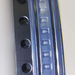
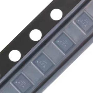
Image for reference only

Manufacturer Part:

SN74LVC1G08DRLR

Package:

SOT-5X3 (1.6 x 1.6 x 0.55 mm)

Brand:

Quality Commitment

Shipping & Payment

Service & Packaging

Product Manual

Other recommendations you may be interested in.

Description

Product Overview

The SN74LVC1G08DRLR from Texas Instruments is a single 2-input AND gate in a 5-pin SOT-5X3 (DRL) surface-mount package. Operating from 1.65V to 5.5V with 3.6ns propagation delay at 3.3V and 32mA output drive, it provides logic AND function with overvoltage-tolerant inputs for mixed-voltage systems.

Key Specifications

Logic Function AND (2-input)
Supply Voltage 1.65V to 5.5V
Propagation Delay 3.6 ns max @ 3.3V
Output Drive +/-32 mA @ 3.3V
Input Voltage Tolerance Up to 5.5V
Quiescent Current 10 uA max
Data Rate 100 Mbps max
Ioff Support Yes (partial power-down)
Operating Temperature -40 to +125 C
Package SOT-5X3 (1.6 x 1.6 mm)

Features

  • Single 2-input positive-AND gate
  • 1.65V to 5.5V wide supply range
  • 5.5V overvoltage-tolerant inputs
  • 3.6ns max propagation delay at 3.3V
  • +/-32mA high output drive
  • 10uA max quiescent current
  • Ioff supports partial power-down
  • 2kV HBM ESD protection
  • Ultra-small 1.6×1.6mm DRL package

Applications

  • Logic gating in mixed-voltage systems
  • Signal enable combining
  • Voltage level translation
  • Industrial and consumer logic
Product Introduction: SN74LVC1G08DRLR Product Introduction

The SN74LVC1G08DRLR from Texas Instruments is a single 2-input positive-AND gate in a 5-pin SOT-5X3 (DRL) surface-mount package. The LVC family provides low-voltage CMOS logic with high output drive while maintaining low static power. The DRL package at 1.6×1.6mm is one of the smallest logic gate packages available. Operating from 1.65V to 5.5V with inputs tolerant to 5.5V regardless of VCC, the device supports mixed-voltage designs where logic levels differ between subsystems. The 3.6ns max propagation delay at 3.3V enables use in high-speed logic paths. The Ioff feature ensures the device does not back-drive the supply rail when VCC is removed, supporting hot-swap and partial power-down applications.

Working Principle: SN74LVC1G08DRLR Working Principle

The SN74LVC1G08 performs the Boolean AND function: Y = A AND B. (1) CMOS Logic: A fully static CMOS implementation uses complementary P-channel and N-channel transistor networks. The AND function is internally implemented as a NAND gate followed by an inverter, minimizing transistor count and propagation delay. (2) Overvoltage-Tolerant Inputs: The input protection diodes are designed to tolerate voltages up to 5.5V regardless of VCC level, allowing the device to receive signals from higher-voltage logic without level shifting. The input leakage current remains within specification with 5.5V applied. (3) Ioff Feature: When VCC is 0V, the Ioff circuitry prevents parasitic current paths from the inputs through the device to the VCC rail. This allows the device to be used in systems where some sections may be powered down while others remain active. (4) Output Drive: The +/-32mA output drive at 3.3V provides robust signal integrity for driving multiple loads or long PCB traces.

Pin Description: SN74LVC1G08DRLR Pin Definition and Functions
Pin Name Type Description
1 B Input Data input B
2 A Input Data input A
3 GND Power Ground
4 Y Output AND gate output (Y = A AND B)
5 VCC Power Supply voltage (1.65-5.5V)
Application Scenarios: In which products and applications is SN74LVC1G08DRLR used
  • Signal enable combining with AND gate requiring both conditions HIGH for activation at 3.3V or 5V
  • Mixed-voltage system with 5V input signals and 3.3V logic supply using overvoltage-tolerant inputs
  • Hot-swap logic with Ioff feature preventing back-drive during partial power-down
  • Space-constrained board with ultra-small 1.6×1.6mm DRL package and 32mA output drive
Alternative Models: What chips are recommended as replacements for SN74LVC1G08DRLR
Model Manufacturer Function Package Notes
SN74LVC1G08DBVR TI AND SOT-23-5 Larger package
SN74LVC1G08DCKR TI AND SC-70-5 Mid-size package
SN74LVC1G08DPWR TI AND X2SON-5 Smallest (0.8×0.8mm)
NC7SZ08P5X onsemi AND SOT-23-5 Pin-compatible

Recommend Parts

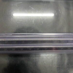
MCP6S26-I

6-channel PGA, SPI interface, gains 1-32V/V, 10MHz BW, rail-to-rail, 2.5-5.5V, SOIC-14

Brand: MICROCHIP

Package: SOIC-14 (150 mils body width)

IN STOCK: 6800pcs

Cargo cycle: 3-7 Days

The minimum order is 1

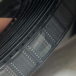
W25Q80VSSI

8Mbit Serial Flash, Quad SPI, 104MHz, SOIC-8, 2.7-3.6V

Brand: Winbond

Package: SOIC-8 208mil (5.3×8.0mm)

IN STOCK: 4316pcs

Cargo cycle: 3-7 Days

The minimum order is 1

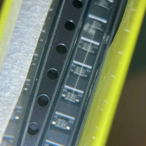
MM3Z9V1

9.1V 200mW Zener diode, SOD-323, onsemi/Diotec

Brand: ON

Package: SOD-323 (2.5 x 1.25 x 0.85 mm)

IN STOCK: 10735pcs

Cargo cycle: 3-7 Days

The minimum order is 1

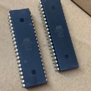
AT89S51

8-bit 8051 MCU, 4KB ISP Flash, 128B RAM, 32 I/O, 2 timers, UART, watchdog timer, dual DPTR, 33MHz, ISP programming, PDIP-40, Atmel AT89S51.

Package: PDIP-40 / TQFP-44 / PLCC-44

IN STOCK: 15000pcs

Cargo cycle: 3-7 Days

The minimum order is 1

GD32F303CBT6

Cortex-M4 32-bit MCU, 120MHz, 128KB Flash, 32KB SRAM, LQFP-48

Brand: gigadevice

Package: LQFP-48 (7x7mm, 0.5mm pitch)

IN STOCK: 3342pcs

Cargo cycle: 3-7 Days

The minimum order is 1

MIC5205-3.3YM5-TR

3.3V 150mA ultra-low-noise LDO, 165mV dropout, 30uVrms noise, SOT-23-5

Brand: MICROCHIP

Package: SOT-23-5 (2.9 x 1.6 x 1.1mm)

IN STOCK: 9858pcs

Cargo cycle: 3-7 Days

The minimum order is 1