
Opens in a new tab

DS90LV031ATMX

Quad LVDS Driver, 400Mbps, 3.3V, SOIC-16

5678

Effective Inventory

Image for reference only

Manufacturer Part:

DS90LV031ATMX

Package:

SOIC-16 (9.9 x 3.9 x 1.75 mm)

Brand:

Quality Commitment

Shipping & Payment

Service & Packaging

Product Manual

Other recommendations you may be interested in.

Description

Product Overview

The DS90LV031ATMX from Texas Instruments is a 3V quad LVDS differential line driver supporting data rates over 400 Mbps, with tri-state outputs and 3.0-3.6V supply in an SOIC-16 package.

Key Specifications

Type Quad LVDS Differential Line Driver
Channels 4
Supply Voltage 3.0 V to 3.6 V
Data Rate 400 Mbps (200 MHz)
Differential Output Voltage 250 mV to 450 mV (typical 350 mV)
Output Offset Voltage 1.125 V to 1.375 V (typical 1.2 V)
Propagation Delay 2.0 ns (typical)
Output Transition Time 0.5 ns (typical)
Package SOIC-16
Operating Temperature -40C to +85C

Features

  • 4 LVDS differential drivers in one package
  • 400+ Mbps data rate (200 MHz clock)
  • 350 mV typical differential output swing
  • 3.0V to 3.6V single supply
  • Tri-state outputs for bus sharing
  • Companion receiver: DS90LV032A
  • Compliant with TIA/EIA-644 (LVDS)

Applications

  • High-speed point-to-point data links
  • Backplane and cable interconnects
  • Video and display data transmission
  • Clock distribution networks
Product Introduction: DS90LV031ATMX Product Introduction

The DS90LV031ATMX from Texas Instruments is a quad CMOS differential line driver designed for applications requiring ultra-low power dissipation and high data rates using Low Voltage Differential Signaling (LVDS) technology. The device accepts LVTTL/LVCMOS input levels and translates them to low-voltage (350mV typical) differential output signals compliant with the TIA/EIA-644 LVDS standard. Data rates in excess of 400 Mbps are supported. The current-mode driver design provides constant 3.5 mA output current that develops 350 mV across a 100-ohm termination resistor at the receiver. The output offset voltage of 1.2V centers the signal within the receiver common-mode range. EN and EN* pins provide tri-state control for bus sharing and ultra-low idle power of 13 mW typical. The DS90LV031A paired with the DS90LV032A receiver provides a complete LVDS communication solution consuming 80% less power than PECL alternatives.

Working Principle: DS90LV031ATMX Working Principle

The DS90LV031ATMX uses a current-mode driver architecture where a controlled 3.5 mA current source is steered through the differential output pair. When the input is HIGH, current flows from the Y output through the 100-ohm termination resistor to the Z output, creating a positive differential voltage. When the input is LOW, the current direction reverses, creating a negative differential voltage. This current-mode approach provides several advantages: the 350 mV swing is relatively constant regardless of load impedance variations, the quiescent current remains flat versus switching frequency (unlike RS-422 voltage-mode drivers), and the low swing minimizes EMI and power dissipation. The output is centered at 1.2V offset from ground, within the 0V to 2.4V LVDS receiver common-mode range. The tri-state function disconnects the current source, reducing supply current to the 3.5 mA idle state. The 2ns propagation delay and 0.5ns transition times enable the 400 Mbps data rate.

Pin Description: DS90LV031ATMX Pin Definition and Functions
Pin Name Type Function
1 DIN1 Input Driver 1 data input
2 DIN2 Input Driver 2 data input
3 DOUT2+ Output Driver 2 positive output
4 DOUT2- Output Driver 2 negative output
5 GND Power Ground
6 DOUT3- Output Driver 3 negative output
7 DOUT3+ Output Driver 3 positive output
8 DIN3 Input Driver 3 data input
9 DIN4 Input Driver 4 data input
10 DOUT4- Output Driver 4 negative output
11 DOUT4+ Output Driver 4 positive output
12 EN Input Enable (active HIGH)
13 EN* Input Enable (active LOW)
14 DOUT1- Output Driver 1 negative output
15 DOUT1+ Output Driver 1 positive output
16 VCC Power 3.3V supply
Application Scenarios: In which products and applications is DS90LV031ATMX used
  • 4-channel high-speed video data link at 400Mbps per channel over Cat-5 cable
  • Backplane clock distribution at 200MHz with LVDS point-to-point topology
  • Multi-drop sensor data acquisition with tri-state bus sharing
  • FPGA-to-ASIC high-speed parallel data transfer with 4 LVDS pairs
Alternative Models: What chips are recommended as replacements for DS90LV031ATMX
Manufacturer Part Number Package Notes
TI DS90LV031ATMX/NOPB SOIC-16 Same device, different packing
ADI ADN4665ARZ SOIC-16 Quad LVDS driver, pin-compatible
ST STLVDS31BDR SOIC-16 Quad LVDS driver, equivalent
TI SN65LVDS31DR SOIC-16 LVDS driver, newer family
TI DS90LV047ATMX SOIC-16 Quad bus LVDS driver, half-duplex

Recommend Parts

MCP6S26-I

6-channel PGA, SPI interface, gains 1-32V/V, 10MHz BW, rail-to-rail, 2.5-5.5V, SOIC-14

Brand: MICROCHIP

Package: SOIC-14 (150 mils body width)

IN STOCK: 6800pcs

Cargo cycle: 3-7 Days

The minimum order is 1

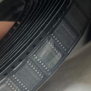
W25Q80VSSI

8Mbit Serial Flash, Quad SPI, 104MHz, SOIC-8, 2.7-3.6V

Brand: Winbond

Package: SOIC-8 208mil (5.3×8.0mm)

IN STOCK: 4316pcs

Cargo cycle: 3-7 Days

The minimum order is 1

MM3Z9V1

9.1V 200mW Zener diode, SOD-323, onsemi/Diotec

Brand: ON

Package: SOD-323 (2.5 x 1.25 x 0.85 mm)

IN STOCK: 10735pcs

Cargo cycle: 3-7 Days

The minimum order is 1

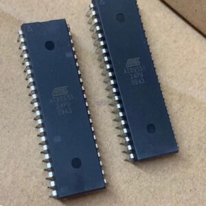
AT89S51

8-bit 8051 MCU, 4KB ISP Flash, 128B RAM, 32 I/O, 2 timers, UART, watchdog timer, dual DPTR, 33MHz, ISP programming, PDIP-40, Atmel AT89S51.

Package: PDIP-40 / TQFP-44 / PLCC-44

IN STOCK: 15000pcs

Cargo cycle: 3-7 Days

The minimum order is 1

GD32F303CBT6

Cortex-M4 32-bit MCU, 120MHz, 128KB Flash, 32KB SRAM, LQFP-48

Brand: gigadevice

Package: LQFP-48 (7x7mm, 0.5mm pitch)

IN STOCK: 3342pcs

Cargo cycle: 3-7 Days

The minimum order is 1

MIC5205-3.3YM5-TR

3.3V 150mA ultra-low-noise LDO, 165mV dropout, 30uVrms noise, SOT-23-5

Brand: MICROCHIP

Package: SOT-23-5 (2.9 x 1.6 x 1.1mm)

IN STOCK: 9858pcs

Cargo cycle: 3-7 Days

The minimum order is 1