
Opens in a new tab

SN74LS138N

3-to-8 decoder/demux, active-low outputs, 3 enables, LS TTL, PDIP-16

14000

Effective Inventory

Image for reference only

Manufacturer Part:

SN74LS138N

Package:

PDIP-16 (19.3 x 6.35 x 4.57mm, 2.54mm pitch, through-hole)

Brand:

Quality Commitment

Shipping & Payment

Service & Packaging

Product Manual

Description

Product Overview

The SN74LS138N is a 3-line to 8-line decoder/demultiplexer from Texas Instruments with 3 enable inputs and inverting outputs in a 16-pin PDIP package.

Key Specifications

Function 3-to-8 decoder/demultiplexer
Logic Family LS (Low-power Schottky)
Supply Voltage 4.75V to 5.25V (5V nominal)
Inputs 3 address (A, B, C) + 3 enable (G1, G2A, G2B)
Outputs 8 active-low (Y0-Y7)
Propagation Delay 22ns typical (address to output)
Enable to Output Delay 18ns typical
Output Low Current (IOL) 8mA
Operating Temperature 0°C to +70°C
Package PDIP-16 (19.3 x 6.35mm)

Features

  • 3-to-8 line decoder with active-low outputs
  • 3 enable inputs: G1 (active high), G2A and G2B (active low)
  • Demultiplexing capability with data input via enable pins
  • Direct replacement for 74138 and 74LS138
  • Input clamp diodes for undershoot protection
  • Multiplex expansion using multiple devices

Applications

  • Memory chip select decoding
  • I/O port address decoding
  • Data demultiplexing
  • Clock distribution and enable generation
  • 7-segment display digit selection
Product Introduction: SN74LS138N Product Introduction

The SN74LS138N from Texas Instruments is a 3-line to 8-line decoder/demultiplexer designed for high-performance memory decoding and data routing. Three binary address inputs (A, B, C) select one of eight active-low outputs (Y0-Y7). The three enable inputs provide flexible control: G1 is active-high, while G2A and G2B are active-low. The device is enabled only when G1 is high AND both G2A and G2B are low. When disabled, all outputs are high (inactive). The active-low outputs directly drive chip-select pins on memory and peripheral ICs without external inverters. As a demultiplexer, data applied to one of the enable inputs is routed to the selected output. Multiple SN74LS138 devices can be cascaded using the enable inputs to expand the decoding range to 4-to-16, 5-to-32, or more. The N suffix denotes the PDIP-16 through-hole package.

Working Principle: SN74LS138N Working Principle

The SN74LS138N decodes a 3-bit binary address into one of eight mutually exclusive active-low outputs. When the device is enabled (G1=HIGH, G2A=LOW, G2B=LOW), the 3-bit address on inputs C, B, A (where C is MSB) selects one output to go LOW while all other outputs remain HIGH. For example, CBA=000 selects Y0 (LOW), CBA=001 selects Y1 (LOW), and so on through CBA=111 selecting Y7 (LOW). The three enable inputs provide cascading capability: a 4-to-16 decoder is built by using the 4th address bit to enable one of two 138 devices (G1 of one device, G2A of the other). For demultiplexing, data is applied to one of the enable pins (e.g., G1) while the other enables are held active; the data signal is then routed to the output selected by the address inputs. The active-low output convention matches the active-low chip-select pins found on most memory and peripheral ICs.

Pin Description: SN74LS138N Pin Definition and Functions
Pin Name Type Description
1 A Input Address input A (LSB)
2 B Input Address input B
3 C Input Address input C (MSB)
4 G2B Input Enable input (active low)
5 G2A Input Enable input (active low)
6 G1 Input Enable input (active high)
7 Y7 Output Decoded output 7 (active low)
8 GND Power Ground
9 Y6 Output Decoded output 6 (active low)
10 Y5 Output Decoded output 5 (active low)
11 Y4 Output Decoded output 4 (active low)
12 Y3 Output Decoded output 3 (active low)
13 Y2 Output Decoded output 2 (active low)
14 Y1 Output Decoded output 1 (active low)
15 Y0 Output Decoded output 0 (active low)
16 VCC Power Supply (4.75V to 5.25V)
Application Scenarios: In which products and applications is SN74LS138N used
  • Memory Decode: 3 address lines generate 8 active-low chip selects for 8 memory-mapped peripherals
  • I/O Port Decode: Cascading two 138s creates a 4-to-16 decoder for 16 I/O ports from 4 address lines
  • Display Select: Active-low outputs directly drive common-cathode 7-segment display digit enables
  • Data Routing: As demultiplexer, routes serial data to one of 8 output destinations under address control
  • Clock Distribution: Routes a clock signal to one of 8 destinations using enable pin as data input
Alternative Models: What chips are recommended as replacements for SN74LS138N
Model Manufacturer Key Difference Package Supply
74LS138N TI/Nexperia Original TTL version with 5V-only supply, typical propagation delay 10-15ns DIP-16 5V TTL
74LS138D TI/Nexperia Surface-mount SOIC version of LS with identical logic function SOIC-16 5V TTL
74HC138D TI/Nexperia CMOS version with wide 2-6V supply range, lower power consumption and higher noise immunity SOIC-16 2-6V CMOS
74HC138N TI/Nexperia Through-hole DIP version of HC family for prototyping and repair DIP-16 2-6V CMOS
74HCT138D TI/Nexperia CMOS with TTL-compatible input levels, ideal for mixing with LS devices at 5V SOIC-16 4.5-5.5V TTL-in
74HCT138N TI/Nexperia Through-hole DIP version of HCT family for prototyping and repair DIP-16 4.5-5.5V TTL-in
74AC138D TI/Nexperia Advanced CMOS with 2-6V supply and higher output drive current (24mA vs 6mA for HC) SOIC-16 2-6V CMOS
74AC138N TI/Nexperia Through-hole DIP version of AC family for prototyping and repair DIP-16 2-6V CMOS
74LVC138D TI/Nexperia Low-voltage CMOS for 1.65-3.6V modern logic with 24mA output drive and bus-hold inputs SOIC-16 1.65-3.6V CMOS
74LVC138N TI/Nexperia Through-hole DIP version of LVC family for prototyping and repair DIP-16 1.65-3.6V CMOS

The 74138 is a 3-Line to 8-Line Decoder/Demultiplexer. Family variants span from the original LS TTL (5V only) to modern LVC/AUP (down to 0.8V). HC and HCT versions offer 2-6V CMOS operation with HCT providing TTL-compatible input thresholds for mixed 5V systems. CD4000-series equivalents offer the widest 3-18V supply range at the cost of lower switching speed. DIP packages (N suffix) are through-hole; SOIC (D suffix) and TSSOP are surface-mount.

Recommend Parts

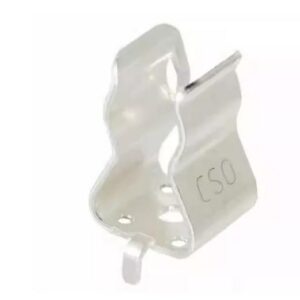
0751.0505

Schurter fuse, 0751.0505

Brand: schurter

Package: See datasheet

IN STOCK: 6768pcs

Cargo cycle: 3-7 Days

The minimum order is 1

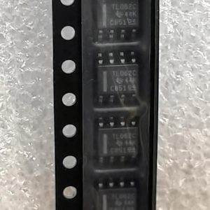
TL062CDR

Low-power JFET-input dual op-amp, 1MHz GBW, 30pA Ibias, SOIC-8, ±3.5V to ±18V

Brand: TI

Package: SOIC-8 (3.9 x 4.9 x 1.75mm)

IN STOCK: 11576pcs

Cargo cycle: 3-7 Days

The minimum order is 1

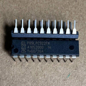
P89LPC922FN

8-bit 80C51 MCU, 8KB Flash, 256B RAM, 20-SSOP

Brand: NXP

Package: SSOP-20 (7.2 x 5.3 mm)

IN STOCK: 12628pcs

Cargo cycle: 3-7 Days

The minimum order is 1

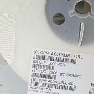
AC0603JR-070RL

Chip Resistor, 0Ω (Zero Ohm Jumper), ±5%, 0603 (1608 Metric), 1/10W (100mW)

Brand: Yageo

Package: 0603 (1608 Metric)

IN STOCK: 100000pcs

Cargo cycle: 3-7 Days

The minimum order is 1

LMR34206FSC5RNXRQ1

42V 2A sync buck, 5V fixed, 2.2MHz, 18uA Iq, AEC-Q100, SOT-563

Brand: TI

Package: SOT-563 (1.6 x 1.2 x 0.55mm)

IN STOCK: 6500pcs

Cargo cycle: 3-7 Days

The minimum order is 1

AO3402

30V N-channel trench MOSFET, SOT-23, 4A, RDS(on) 52m ohm max @ 10V, Qg 10nC, 2.5V gate drive capable, -55C to +150C.

Brand: aosmd

Package: SOT-23 (2.9 x 1.6 x 1.25mm)

IN STOCK: 14066pcs

Cargo cycle: 3-7 Days

The minimum order is 1