
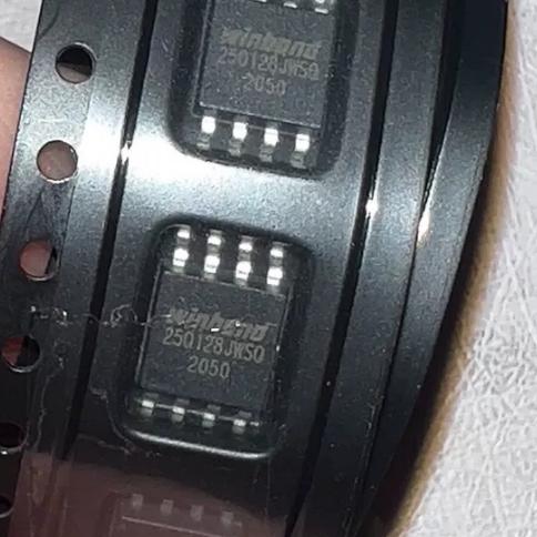





The W25Q128JVSIQ is a 128Mbit (16MB) SPI NOR Flash from Winbond in SOIC-8 208-mil (5.3×5.3mm). Supports Standard/Dual/Quad SPI up to 133MHz (532MHz effective Quad I/O, 66MB/s throughput). Organized as 65,536 pages of 256 bytes; 4,096 x 4KB sectors, 256 x 64KB blocks. Page program: 3ms. Supply: 2.7-3.6V. Active: 25mA, standby: 15uA, power-down: less than 1uA. 100K P/E cycles, 20-year retention. Unique 64-bit ID, 3×256-byte OTP security registers, SFDP. -40C to +85C. MSL-3, RoHS3, ECCN 3A991B1A. Tube packaging.
Home » Flash Memory (NAND / NOR Flash), Integrated Circuits ICs » W25Q128JVSIQ
W25Q128JVSIQ
128Mbit SPI NOR Flash, Standard/Dual/Quad SPI, 133MHz, SOIC-8, -40~85C, 100K cycles
127946
Effective Inventory
Manufacturer Part:
W25Q128JVSIQ
Package:
SOIC-8 208-mil (5.3 x 5.3 x 1.8 mm)
Brand:
Product Categories:
Quality Commitment
Shipping & Payment
Service & Packaging
Product Manual
Other recommendations you may be interested in.
Description
Product Introduction: W25Q128JVSIQ Product Introduction
The W25Q128JVSIQ is a 128M-bit (16M-byte) serial NOR Flash memory device from Winbond Electronics, housed in an 8-pin SOIC 208-mil package. It is part of the SpiFlash family and supports Standard SPI, Dual SPI, and Quad SPI interfaces, providing flexible and high-speed data access for code storage, data logging, and execute-in-place (XIP) applications.
The memory array is organized as 65,536 programmable pages of 256 bytes each. The device supports flexible erase granularity: 4 KB sectors (4,096 total), 32 KB blocks, 64 KB blocks (256 total), and full chip erase. Page programming time is typically 3 ms, and block erase time is approximately 120 ms for a 32 KB block.
The SPI clock frequency supports up to 133 MHz, enabling equivalent data rates of 266 MHz in Dual I/O mode and 532 MHz in Quad I/O mode. In Quad SPI mode at 133 MHz, the effective data throughput can reach 66 MB/s, surpassing many parallel Flash memories. The device also supports SPI Mode 0 (CPOL=0, CPHA=0) and Mode 3 (CPOL=1, CPHA=1).
The operating voltage range is 2.7V to 3.6V, compatible with standard 3.3V logic systems. Active read current is typically 25 mA at 133 MHz. Standby current is typically 15 uA, and power-down current drops to less than 1 uA, making the device suitable for battery-powered applications.
Security features include: software and hardware write protection, power-up/down data protection, volatile and non-volatile lock bits for sector protection, 256-byte One-Time Programmable (OTP) security register, unique 64-bit serial number for device identification, and three 256-byte security registers for user data storage. The Serial Flash Discoverable Parameters (SFDP) register facilitates automatic software detection and configuration.
The device supports program/erase suspend and resume operations, allowing interruption of long erase operations for higher-priority reads. The continuous read mode supports configurable wrap lengths of 8, 16, 32, and 64 bytes for cache optimization.
The W25Q128JVSIQ is qualified for 100,000 program/erase cycles per sector with a 20-year data retention specification. The operating temperature range is -40C to +85C (industrial grade). The device is RoHS3 compliant, MSL Level 3 (168 hours), and classified as ECCN 3A991B1A. Tube packaging is standard.
The JV variant represents the latest generation of the W25Q128 family, featuring enhanced SPI modes and improved performance over earlier JQ and JM variants. The SIQ suffix denotes SOIC-8 package, industrial temperature range, and tube packaging.
Working Principle: W25Q128JVSIQ Working Principle
The W25Q128JVSIQ operates as a serial NOR Flash memory controlled through SPI-compatible command sequences issued by a host microcontroller or SoC.
Memory Architecture: The 128M-bit (16M-byte) array is organized as a flat address space from 000000h to FFFFFFh (24-bit addressing). The array is hierarchically divided into: 256 bytes per page (65,536 pages total), 16 pages per 4 KB sector (4,096 sectors total), and 256 pages per 64 KB block (256 blocks total). This layered structure allows flexible erase granularity: a single 4 KB sector can be erased independently, while larger blocks or the entire chip can be erased for bulk operations.
SPI Command Protocol: The host communicates with the device by asserting /CS low, clocking in an 8-bit command opcode on DI (IO0), followed by address bytes and data bytes as required by the specific command. Data is shifted in on the rising edge of CLK and shifted out on the falling edge. Each command sequence ends by deasserting /CS high. Standard read commands use DI for data input and DO for data output. In Dual SPI mode, both IO0 and IO1 serve as bidirectional data lines. In Quad SPI mode, all four IO lines (IO0-IO3) carry data simultaneously, quadrupling throughput.
Write Operations: Before writing data, the target memory region must first be erased (all bits set to 1). The Page Program command (02h) writes up to 256 bytes of data within a single page boundary. Data written across page boundaries wraps to the beginning of the same page, so multiple page program operations are required for larger data sets. The Write Enable command (06h) must be issued before any program or erase operation. The Status Register WEL (Write Enable Latch) bit must be set before the device accepts write commands.
Erase Operations: Four erase commands are available: Sector Erase (20h, 4 KB), Block Erase 32KB (52h), Block Erase 64KB (D8h), and Chip Erase (C7h/60h). Erase operations set all bits in the target region to 1 (logic HIGH). Typical erase times are: sector erase 45 ms (max 200 ms), 32 KB block erase 120 ms, 64 KB block erase 150 ms, and chip erase 40 seconds (max 200 seconds).
Suspend/Resume: The Program/Erase Suspend command (75h) allows interruption of an in-progress program or erase operation so that data can be read from a different area of memory. The Program/Erase Resume command (7Ah) restarts the suspended operation. This feature enables real-time data access during long erase cycles.
Protection Mechanisms: Write protection is controlled through Status Register bits and lock-down mechanisms. The /WP pin (IO2) can be used to hardware-protect the Status Register, preventing accidental changes to protection settings. Individual sector protection is available through the Block Protect bits (BP3-BP0) in Status Registers. Once set, the Sector Lock-Down function permanently prevents modification of protection settings for selected sectors.
Power Management: The device supports Deep Power-Down mode entered via command B9h, reducing current consumption to less than 1 uA. Exit from power-down requires the Release from Deep Power-Down command (ABh) followed by a delay of 3 us minimum. During power-up, the device automatically enters standby mode and /CS must be held HIGH during the power ramp to prevent spurious commands.
Pin Description: W25Q128JVSIQ Pin Definition and Functions
| Pin | Name | Type | Description |
|---|---|---|---|
| 1 | /CS | Input | Chip Select; active LOW; must be driven HIGH during power-up and power-down; selects the device for SPI communication |
| 2 | DO (IO1) | Output / I/O | Data Output in Standard SPI; bidirectional IO1 in Dual/Quad SPI; serial data output on falling CLK edge; high-impedance when /CS is HIGH |
| 3 | /WP (IO2) | Input / I/O | Write Protect in Standard SPI; active LOW; protects Status Register bits; bidirectional IO2 in Quad SPI mode |
| 4 | GND | Power | Ground; connect to PCB ground plane |
| 5 | DI (IO0) | Input / I/O | Data Input in Standard SPI; bidirectional IO0 in Dual/Quad SPI; serial data input on rising CLK edge |
| 6 | CLK | Input | Serial Clock; SPI clock input; data input sampled on rising edge; data output driven on falling edge; up to 133 MHz |
| 7 | /HOLD (IO3) | Input / I/O | Hold in Standard SPI; active LOW; pauses serial communication without deselecting device; bidirectional IO3 in Quad SPI; can be configured as /RESET via Status Register |
| 8 | VCC | Power | Power supply; 2.7V to 3.6V operating range; bypass with 0.1 uF ceramic capacitor to GND close to pin |
Application Scenarios: In which products and applications is W25Q128JVSIQ used
| Application | Description |
|---|---|
| Embedded System Code Storage | Stores MCU/SoC firmware for boot-up; XIP capability allows direct code execution without shadowing to RAM; Quad SPI mode provides sufficient bandwidth for real-time code access |
| Firmware OTA Updates | Dual-bank or sector-based update strategy; 4 KB sector erase granularity minimizes flash wear during frequent updates; suspend/resume allows system operation during update |
| Data Logging and Configuration | Non-volatile storage for sensor data logs, calibration parameters, and device configuration; 100K cycle endurance supports frequent writes; OTP register for permanent calibration data |
| Consumer Electronics | Firmware and asset storage in smart speakers, IoT devices, networking equipment, and set-top boxes; low 1 uA power-down current extends battery life in portable devices |
| Industrial Control Systems | Program storage for PLCs, motor controllers, and industrial gateways; -40C to +85C temperature range meets industrial requirements; SFDP register enables automatic device detection |
Alternative Models: What chips are recommended as replacements for W25Q128JVSIQ
| Model | Manufacturer | Compatibility | Key Difference |
|---|---|---|---|
| W25Q128JVSSIQ | Winbond | Pin-Compatible / Same Die | WSON-8 6x5mm package; same 128Mbit capacity and SPI interface; smaller footprint for space-constrained designs; requires thermal pad on PCB |
| MX25L12833FMI-10G | Macronix | Pin-Compatible / Software Compatible | 128Mbit SPI NOR Flash; SOIC-8; 133 MHz; command-set compatible; different SFDP parameters; verify JEDEC ID (C2h 20h 18h vs EFh 40h 18h) |
| S25FL128LAGMFI01 | Infineon (Cypress) | Software Compatible | 128Mbit SPI NOR Flash; different command set extensions; verify software driver compatibility; similar performance specifications |
| GD25Q128C | GigaDevice | Pin-Compatible / Software Compatible | 128Mbit SPI NOR Flash; SOIC-8; 120 MHz; widely used as cost-effective alternative; verify specific timing parameters for critical applications |
| W25Q256JVSIQ | Winbond | Pin-Compatible / Same Family | 256Mbit (32 MB) capacity; same SOIC-8 footprint; uses 4-byte address commands for full address space; software-compatible with address extension |
Recommend Parts

ISL95855HRTZ-T
IMVP8 3+2+1 phase buck controller, R3 technology, 4.5-25V input, 48-TQFN
Brand: Renesas
Package: 48-TQFN (6×6 mm, exposed pad)
IN STOCK: 2156pcs
Cargo cycle: 3-7 Days
The minimum order is 1

IRFB4019PBF
150V N-Channel HEXFET Power MOSFET, 47A, 34 mΩ RDS(on), TO-220AB
Brand: infineon
Package: TO-220AB
IN STOCK: 2409pcs
Cargo cycle: 3-7 Days
The minimum order is 1

MSP430F247TPMR
TI MSP430 MCU, 16-bit RISC, 92KB Flash, 8KB RAM, 16MHz, LQFP-64
Brand: texas-instruments
Package: See datasheet
IN STOCK: 13371pcs
Cargo cycle: 3-7 Days
The minimum order is 1

UCC28740DR
CVCC Flyback Controller, 700V startup, opto feedback, <10mW no-load, SOIC-7
Brand: TI
Package: SOIC-7 (4.9 x 3.9 x 1.75 mm)
IN STOCK: 4840pcs
Cargo cycle: 3-7 Days
The minimum order is 1

MMUN2211LT1G
NPN digital transistor, R1=10kΩ R2=10kΩ, 50V, 100mA, SOT-23-3, pre-biased BRT switch
Brand: Onsemi
Package: SOT-23-3 (TO-236, SC-59)
IN STOCK: 8500pcs
Cargo cycle: 3-7 Days
The minimum order is 1

PIC32MX795F512L-80I/PF
32-bit PIC32MX MCU with Ethernet/CAN/USB, 80MHz, 512KB Flash, TQFP-100, industrial
Brand: MICROCHIP
Package: TQFP-100 (14 x 14 mm)
IN STOCK: 7912pcs
Cargo cycle: 3-7 Days
The minimum order is 1