

Opens in a new tab

CD4066BE

Quad bilateral analog switch, 125Ω RON, 40MHz, 3-18V, PDIP-14

6000

Effective Inventory

Image for reference only

Manufacturer Part:

CD4066BE

Package:

PDIP-14 (19.3 x 6.35 x 4.57mm, 2.54mm pitch, through-hole)

Brand:

Quality Commitment

Shipping & Payment

Service & Packaging

Product Manual

Description

Product Overview

The CD4066BE from Texas Instruments is a CMOS quad bilateral switch with 125Ω on-state resistance, 10pA off-state leakage, and 40MHz bandwidth, pin-compatible with CD4016B in a 14-pin PDIP package.

Key Specifications

Number of Switches 4 (independent SPST)
Supply Voltage 3V to 18V
On-State Resistance 125Ω typical @ VDD=15V, 470Ω @ VDD=5V
On-Resistance Matching Within 5Ω @ VDD=15V
Off-State Leakage 10pA typical @ VDD=10V
Signal Range Full VDD swing (0V to VDD)
Bandwidth (On) 40MHz typical
Crosstalk -50dB typical @ 8MHz
Distortion <0.5% typical @ 1kHz, 5Vp-p
Control Input Impedance 10^12 Ω typical
On/Off Ratio 80dB typical @ 10kHz
Operating Temperature -55°C to +125°C
Package PDIP-14 (19.3 x 6.35mm)

Features

  • Four independent bilateral (bidirectional) switches
  • Pin-compatible with CD4016B (lower RON)
  • 125Ω on-state resistance @ 15V
  • Ultra-low off-state leakage: 10pA typical
  • Flat on-resistance over full signal range
  • High linearity: <0.5% distortion
  • 40MHz bandwidth

Applications

  • Analog signal switching and multiplexing
  • Programmable gain amplifier
  • Digital control of analog signals
  • Sample-and-hold (CD4016B preferred)
  • Chopper/modulator circuits
Product Introduction: CD4066BE Product Introduction

The CD4066BE from Texas Instruments is a quad bilateral (bidirectional) analog switch containing four independent single-pole single-throw (SPST) switches in a 14-pin PDIP package. Each switch is controlled by a separate active-HIGH enable input; when the control is HIGH, the switch is ON (conducting), and when LOW, the switch is OFF (high impedance). The 125Ω typical on-state resistance at VDD=15V is significantly lower than the older CD4016B (which has ~400Ω), and the on-resistance remains relatively flat over the full signal input range (0V to VDD) due to the internal biasing of the n-channel well. The bilateral nature means signals can flow in either direction through the switch — there is no designated input or output. The 10pA off-state leakage is extremely low, making the 4066 suitable for high-impedance signal routing. The 40MHz bandwidth supports audio and medium-frequency signal switching. The BE suffix denotes the PDIP-14 package with full temperature range (-55°C to +125°C).

Working Principle: CD4066BE Working Principle

Each switch in the CD4066BE consists of a parallel pair of PMOS and NMOS transistors (transmission gate) controlled by complementary gate signals. When the control input is HIGH (at VDD), the NMOS gate is driven HIGH and the PMOS gate is driven LOW (via internal inverter), turning both transistors ON and creating a low-resistance path between the two signal terminals. When the control is LOW, both transistors are OFF and the signal path is open (high impedance). The parallel NMOS+PMOS structure ensures that the on-resistance remains relatively constant over the full signal range: the NMOS conducts well for signals near VSS, while the PMOS conducts well for signals near VDD. The internal well-biasing circuit connects the n-channel substrate to the input (when ON) or to VSS (when OFF), eliminating threshold voltage modulation that would cause on-resistance variation with signal level. The control input has extremely high impedance (10^12Ω), drawing negligible current from the driving logic. Since the switch is bilateral, either terminal can be the input or output — the signal can pass in either direction. The 10pA off-state leakage means virtually no signal passes when the switch is open, giving 80dB on/off ratio at 10kHz.

Pin Description: CD4066BE Pin Definition and Functions
Pin Name Type Description
1 1IN/OUT Bidirectional Switch 1 signal terminal A
2 1OUT/IN Bidirectional Switch 1 signal terminal B
3 2OUT/IN Bidirectional Switch 2 signal terminal B
4 2IN/OUT Bidirectional Switch 2 signal terminal A
5 2CTRL Input Switch 2 control (HIGH=ON)
6 3CTRL Input Switch 3 control (HIGH=ON)
7 VSS Power Ground (0V)
8 3IN/OUT Bidirectional Switch 3 signal terminal A
9 3OUT/IN Bidirectional Switch 3 signal terminal B
10 4OUT/IN Bidirectional Switch 4 signal terminal B
11 4IN/OUT Bidirectional Switch 4 signal terminal A
12 4CTRL Input Switch 4 control (HIGH=ON)
13 1CTRL Input Switch 1 control (HIGH=ON)
14 VDD Power Positive supply (3V to 18V)
Application Scenarios: In which products and applications is CD4066BE used
  • 4-Channel Mux: Four inputs to one output (common terminal); MCU controls one switch at a time; selects one of 4 analog signals
  • PGA (Programmable Gain): Switches select different feedback resistors around an op-amp; digital control sets gain
  • Audio Switch: Routes audio signals between sources; low distortion (<0.5%) preserves audio quality
  • Chopper: Switch toggles at high frequency, alternately connecting and disconnecting signal; creates amplitude modulation
  • Logic-Level Mux: Switches digital signals between circuits; 40MHz bandwidth supports moderate-speed digital
Alternative Models: What chips are recommended as replacements for CD4066BE
Model Manufacturer Key Difference Package Supply
CD4066BM TI SOIC-14 surface-mount version with identical logic function and 3-18V range SOIC-14 3-18V
CD4066BE TI Through-hole DIP version for prototyping and legacy board repair DIP-14 3-18V
HEF4066BT NXP Pin-compatible CMOS version with improved ESD protection and 3-15V supply SOIC-14 3-15V
MC144066BDR2G onsemi Pin-compatible equivalent with RoHS compliance and AEC-Q100 automotive option SOIC-14 3-18V
74HC4066D TI/Nexperia HC CMOS version with higher speed and 2-6V supply for modern logic systems SOIC-14 2-6V
74HC4066N TI/Nexperia HC CMOS through-hole version for prototyping with 2-6V supply range DIP-14 2-6V
74HCT4066D Nexperia HCT version with TTL-compatible inputs for mixed 5V TTL/CMOS systems SOIC-14 4.5-5.5V

CD4066 is the CMOS 4000-series quad bilateral switch operating over the wide 3-18V supply range. The HEF4066 (NXP) and MC144066 (onsemi) are direct pin-compatible equivalents. For higher speed at the cost of narrower voltage range, the 74HC4066 HC/HCT families offer significantly faster propagation delay and lower power consumption at 2-6V. Surface-mount versions use the BM/M suffix (SOIC); through-hole versions use the BE suffix (DIP).

Recommend Parts

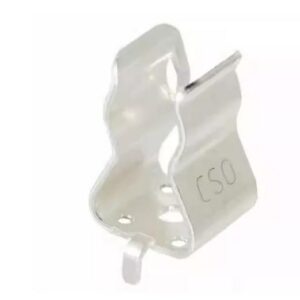
0751.0505

Schurter fuse, 0751.0505

Brand: schurter

Package: See datasheet

IN STOCK: 6768pcs

Cargo cycle: 3-7 Days

The minimum order is 1

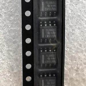
TL062CDR

Low-power JFET-input dual op-amp, 1MHz GBW, 30pA Ibias, SOIC-8, ±3.5V to ±18V

Brand: TI

Package: SOIC-8 (3.9 x 4.9 x 1.75mm)

IN STOCK: 11576pcs

Cargo cycle: 3-7 Days

The minimum order is 1

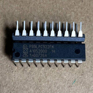
P89LPC922FN

8-bit 80C51 MCU, 8KB Flash, 256B RAM, 20-SSOP

Brand: NXP

Package: SSOP-20 (7.2 x 5.3 mm)

IN STOCK: 12628pcs

Cargo cycle: 3-7 Days

The minimum order is 1

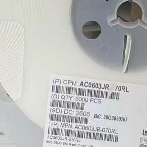
AC0603JR-070RL

Chip Resistor, 0Ω (Zero Ohm Jumper), ±5%, 0603 (1608 Metric), 1/10W (100mW)

Brand: Yageo

Package: 0603 (1608 Metric)

IN STOCK: 100000pcs

Cargo cycle: 3-7 Days

The minimum order is 1

LMR34206FSC5RNXRQ1

42V 2A sync buck, 5V fixed, 2.2MHz, 18uA Iq, AEC-Q100, SOT-563

Brand: TI

Package: SOT-563 (1.6 x 1.2 x 0.55mm)

IN STOCK: 6500pcs

Cargo cycle: 3-7 Days

The minimum order is 1

AO3402

30V N-channel trench MOSFET, SOT-23, 4A, RDS(on) 52m ohm max @ 10V, Qg 10nC, 2.5V gate drive capable, -55C to +150C.

Brand: aosmd

Package: SOT-23 (2.9 x 1.6 x 1.25mm)

IN STOCK: 14066pcs

Cargo cycle: 3-7 Days

The minimum order is 1