
Opens in a new tab

SN74LS151N

8-to-1 data selector/multiplexer, LS TTL, complementary outputs, PDIP-16

5000

Effective Inventory

Image for reference only

Manufacturer Part:

SN74LS151N

Package:

PDIP-16 (19.3 x 6.35 x 4.57mm, 2.54mm pitch, through-hole)

Brand:

Quality Commitment

Shipping & Payment

Service & Packaging

Product Manual

Description

Product Overview

The SN74LS151N from Texas Instruments is an 8-line to 1-line data selector/multiplexer with complementary outputs and active-LOW strobe, capable of selecting one-of-eight data sources or implementing any 4-variable Boolean function in a 16-pin PDIP package.

Key Specifications

Function 8-line to 1-line data selector/multiplexer
Logic Family LS (Low-power Schottky)
Supply Voltage 4.75V to 5.25V (5V nominal)
Data Inputs D0–D7 (8 lines)
Select Inputs S0, S1, S2 (3-bit binary address)
Outputs Y (true) and W (complementary)
Strobe (Enable) Active LOW (G enables outputs)
Propagation Delay (Data→Y) 12ns typical
Propagation Delay (Select→Y) 18–37ns typical
Output Drive (IOL/IOH) 8mA / -0.4mA
Supply Current 6–10mA typical
Operating Temperature 0°C to +70°C
Package PDIP-16 (19.3 x 6.35mm)

Features

  • Selects one-of-eight data lines
  • Complementary Y and W outputs
  • Active-LOW strobe for enabling/disabling
  • Parallel-to-serial conversion capability
  • Can implement any 4-variable Boolean function
  • Input clamp diodes simplify system design

Applications

  • Data routing and selection
  • Parallel-to-serial conversion
  • Boolean function generation
  • GPIO expansion for microcontrollers
  • Address decoding
Product Introduction: SN74LS151N Product Introduction

The SN74LS151N from Texas Instruments is an 8-line to 1-line data selector/multiplexer built with LS TTL technology. It uses three select inputs (S0, S1, S2) to route one of eight data inputs (D0–D7) to the Y output, with the complementary signal available at W. The strobe (G) input, when HIGH, forces Y LOW and W HIGH regardless of other inputs — effectively disabling the device. The 74151 is more than a simple multiplexer: with the eight data inputs tied HIGH or LOW in specific patterns, it can implement any Boolean function of four variables (the three select lines plus the strobe form the four inputs). This makes it a universal logic function generator. For data routing, the 74151 consolidates up to eight signal sources into a single line, reducing pin count on microcontrollers. The N suffix denotes the PDIP-16 through-hole package.

Working Principle: SN74LS151N Working Principle

The SN74LS151N implements the logic function: Y = G · (D0·S0’·S1’·S2′ + D1·S0·S1’·S2′ + D2·S0’·S1·S2′ + D3·S0·S1·S2′ + D4·S0’·S1’·S2 + D5·S0·S1’·S2 + D6·S0’·S1·S2 + D7·S0·S1·S2). When G is LOW (enabled), the 3-bit binary address on S0–S2 selects which data input appears at Y; W is always the complement of Y. When G is HIGH, Y=0 and W=1 regardless of data and select inputs. For data multiplexing: if S2S1S0 = 101 (binary 5), then Y = D5 (the data on input 5). For Boolean function generation: each data input Di is tied to either VCC (1) or GND (0) to represent the desired truth table output for that minterm. For example, to implement the XOR of S0 and S1 (with S2=G=0): set D0=0, D1=1, D2=1, D3=0, D4–D7=don’t care. Then Y = S0’·S1’·0 + S0·S1’·1 + S0’·S1·1 + S0·S1·0 = S0⊕S1.

Pin Description: SN74LS151N Pin Definition and Functions
Pin Name Type Description
1 D3 Input Data input 3
2 D2 Input Data input 2
3 D1 Input Data input 1
4 D0 Input Data input 0
5 Y Output Multiplexer output (true)
6 W Output Complementary multiplexer output
7 G Input Strobe/Enable (active LOW)
8 GND Power Ground
9 S2 Input Select input 2 (MSB)
10 S1 Input Select input 1
11 S0 Input Select input 0 (LSB)
12 D7 Input Data input 7
13 D6 Input Data input 6
14 D5 Input Data input 5
15 D4 Input Data input 4
16 VCC Power Supply (5V)

SN74LS151N uses the PDIP-16 package: VCC at Pin 16, GND at Pin 8. The 8 data inputs (D0-D7) are on Pins 4-1, 15, 14, 13, 12 respectively. Three select lines (A/B/C) on Pins 11, 10, 9 choose which input appears at the outputs. Pin 5 = Y output (true), Pin 6 = W output (complement). Pin 7 = Strobe (active-low enable). When Strobe is HIGH, Y is forced LOW and W is forced HIGH regardless of select inputs. The complementary outputs (Y and W) eliminate the need for an external inverter in many applications. For HC version with wider voltage range, 74HC151 provides the same pinout at 2-6V supply.

Application Scenarios: In which products and applications is SN74LS151N used
  • 8-Channel Data Selector: 8 sensor outputs → D0–D7; MCU 3 GPIOs → S0–S2; G=GND; Y → MCU ADC input; scan channels by changing S0–S2
  • Parallel-to-Serial: 8-bit parallel data on D0–D7; counter on S0–S2; Y outputs one bit per clock; serializes 8-bit word
  • Function Generator: Tie D0–D7 to VCC/GND per truth table; S0–S2 are function inputs; Y = Boolean function of 3 variables
  • 16-to-1 Mux: Two 74151 chips; MSB selects which chip via G; combine Y outputs with AND gate; selects 1 of 16 lines
Alternative Models: What chips are recommended as replacements for SN74LS151N
Model Manufacturer Key Difference Package Supply
74LS151N TI/Nexperia Original TTL version with 5V-only supply, typical propagation delay 10-15ns DIP-16 5V TTL
74LS151D TI/Nexperia Surface-mount SOIC version of LS with identical logic function SOIC-16 5V TTL
74HC151D TI/Nexperia CMOS version with wide 2-6V supply range, lower power consumption and higher noise immunity SOIC-16 2-6V CMOS
74HC151N TI/Nexperia Through-hole DIP version of HC family for prototyping and repair DIP-16 2-6V CMOS
74HCT151D TI/Nexperia CMOS with TTL-compatible input levels, ideal for mixing with LS devices at 5V SOIC-16 4.5-5.5V TTL-in
74HCT151N TI/Nexperia Through-hole DIP version of HCT family for prototyping and repair DIP-16 4.5-5.5V TTL-in
74AC151D TI/Nexperia Advanced CMOS with 2-6V supply and higher output drive current (24mA vs 6mA for HC) SOIC-16 2-6V CMOS
74AC151N TI/Nexperia Through-hole DIP version of AC family for prototyping and repair DIP-16 2-6V CMOS

The 74151 is a 8-Line to 1-Line Data Selector/Multiplexer. Family variants span from the original LS TTL (5V only) to modern LVC/AUP (down to 0.8V). HC and HCT versions offer 2-6V CMOS operation with HCT providing TTL-compatible input thresholds for mixed 5V systems. CD4000-series equivalents offer the widest 3-18V supply range at the cost of lower switching speed. DIP packages (N suffix) are through-hole; SOIC (D suffix) and TSSOP are surface-mount.

Recommend Parts

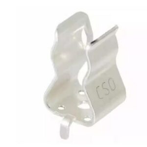
0751.0505

Schurter fuse, 0751.0505

Brand: schurter

Package: See datasheet

IN STOCK: 6768pcs

Cargo cycle: 3-7 Days

The minimum order is 1

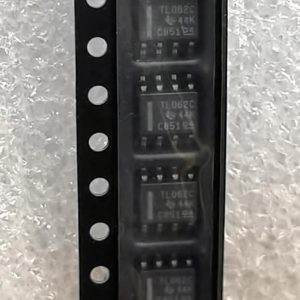
TL062CDR

Low-power JFET-input dual op-amp, 1MHz GBW, 30pA Ibias, SOIC-8, ±3.5V to ±18V

Brand: TI

Package: SOIC-8 (3.9 x 4.9 x 1.75mm)

IN STOCK: 11576pcs

Cargo cycle: 3-7 Days

The minimum order is 1

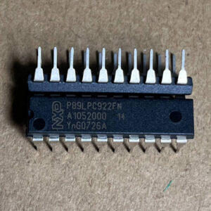
P89LPC922FN

8-bit 80C51 MCU, 8KB Flash, 256B RAM, 20-SSOP

Brand: NXP

Package: SSOP-20 (7.2 x 5.3 mm)

IN STOCK: 12628pcs

Cargo cycle: 3-7 Days

The minimum order is 1

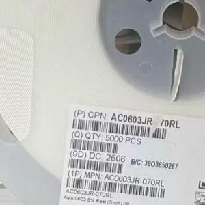
AC0603JR-070RL

Chip Resistor, 0Ω (Zero Ohm Jumper), ±5%, 0603 (1608 Metric), 1/10W (100mW)

Brand: Yageo

Package: 0603 (1608 Metric)

IN STOCK: 100000pcs

Cargo cycle: 3-7 Days

The minimum order is 1

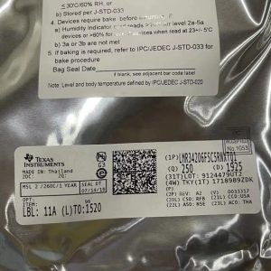
LMR34206FSC5RNXRQ1

42V 2A sync buck, 5V fixed, 2.2MHz, 18uA Iq, AEC-Q100, SOT-563

Brand: TI

Package: SOT-563 (1.6 x 1.2 x 0.55mm)

IN STOCK: 6500pcs

Cargo cycle: 3-7 Days

The minimum order is 1

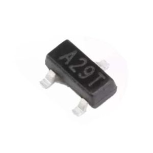
AO3402

30V N-channel trench MOSFET, SOT-23, 4A, RDS(on) 52m ohm max @ 10V, Qg 10nC, 2.5V gate drive capable, -55C to +150C.

Brand: aosmd

Package: SOT-23 (2.9 x 1.6 x 1.25mm)

IN STOCK: 14066pcs

Cargo cycle: 3-7 Days

The minimum order is 1