
Opens in a new tab

CD40106BE

Hex Schmitt-trigger inverter, CMOS 3-18V, hysteresis, PDIP-14

10000

Effective Inventory

Image for reference only

Manufacturer Part:

CD40106BE

Package:

PDIP-14 (19.3 x 6.35 x 4.57mm, 2.54mm pitch, through-hole)

Brand:

Quality Commitment

Shipping & Payment

Service & Packaging

Product Manual

Description

Product Overview

The CD40106BE from Texas Instruments contains six independent Schmitt-trigger inverters with hysteresis, capable of squaring up slowly-changing signals and debouncing mechanical contacts in a 14-pin PDIP package.

Key Specifications

Number of Gates 6 (hex Schmitt-trigger inverter)
Technology CD4000B CMOS
Supply Voltage 3V to 18V
Positive-Going Threshold (VT+) 5.4V typical @ VDD=10V
Negative-Going Threshold (VT−) 3.6V typical @ VDD=10V
Hysteresis (VT+ − VT−) 1.8V typical @ VDD=10V
Propagation Delay 90ns typical @ VDD=10V
Operating Temperature -55°C to +125°C
Package PDIP-14 (19.3 x 6.35mm)

Features

  • Six Schmitt-trigger inverters
  • Wide hysteresis: ~0.2×VDD
  • 3V to 18V supply range
  • Squares slowly-changing waveforms
  • No input rise/fall time requirement

Applications

  • Signal conditioning (square-up)
  • Mechanical switch debounce
  • RC oscillator
  • Level detection
  • Pulse shaping
Product Introduction: CD40106BE Product Introduction

The CD40106BE from Texas Instruments contains six independent Schmitt-trigger inverters. Unlike standard inverters (CD4069), Schmitt-trigger inputs have two distinct threshold voltages: a higher threshold (VT+) for the low-to-high transition and a lower threshold (VT−) for the high-to-low transition. The difference (VT+ − VT−) is the hysteresis, typically 1.8V at VDD=10V. This hysteresis makes the CD40106 immune to noise on slowly-changing input signals: once the output switches, the input must change by the full hysteresis voltage (not just a few millivolts of noise) to cause another output transition. This is essential for squaring up sine waves, triangle waves, and other slowly-rising signals that would cause standard gates to oscillate near the threshold. The CD40106 also has no rise/fall time requirement on its input — signals with unlimited transition times are cleanly converted to sharp square waves. The BE suffix denotes the PDIP-14 package with full temperature range.

Working Principle: CD40106BE Working Principle

Each Schmitt-trigger inverter in the CD40106BE has two switching thresholds. When the input voltage rises from 0V, the output remains HIGH until the input exceeds VT+ (the positive-going threshold, ~5.4V at VDD=10V), at which point the output snaps LOW. When the input falls from VDD, the output remains LOW until the input drops below VT− (the negative-going threshold, ~3.6V at VDD=10V), at which point the output snaps HIGH. The 1.8V hysteresis band between VT− and VT+ means that any noise smaller than 1.8V cannot cause false switching. For debouncing: a mechanical switch connected to the input through a pull-up resistor produces multiple transitions as the contacts bounce; the hysteresis filters these bounces and produces a single clean edge at the output. For RC oscillators: connect the output through a resistor to the input, and a capacitor from input to ground. The capacitor charges through the resistor until it reaches VT+, the output goes LOW, the capacitor discharges until it reaches VT−, the output goes HIGH, and the cycle repeats. Frequency ≈ 1/(0.6 × R × C) at VDD=10V.

Pin Description: CD40106BE Pin Definition and Functions
Pin Name Type Description
1 1A Input Gate 1 input
2 1Y Output Gate 1 output (inverted)
3 2A Input Gate 2 input
4 2Y Output Gate 2 output (inverted)
5 3A Input Gate 3 input
6 3Y Output Gate 3 output (inverted)
7 VSS Power Ground
8 4Y Output Gate 4 output (inverted)
9 4A Input Gate 4 input
10 5Y Output Gate 5 output (inverted)
11 5A Input Gate 5 input
12 6Y Output Gate 6 output (inverted)
13 6A Input Gate 6 input
14 VDD Power Supply (3V to 18V)

CD40106BE uses the PDIP-14 package with hex inverter pinout: VDD at Pin 14, VSS at Pin 7. Six independent Schmitt-trigger inverters: Inv 1 (Pin 1 in, Pin 2 out), Inv 2 (Pin 3 in, Pin 4 out), Inv 3 (Pin 5 in, Pin 6 out), Inv 4 (Pin 9 in, Pin 8 out), Inv 5 (Pin 11 in, Pin 10 out), Inv 6 (Pin 13 in, Pin 12 out). The Schmitt-trigger hysteresis (typ 2V at 5V supply) makes this device ideal for noise rejection on slowly changing signals, switch debouncing, and oscillator circuits. For 74HC equivalent with faster switching, use 74HC14 (same pinout, 2-6V supply). The CD40106B hysteresis is supply-voltage proportional.

Application Scenarios: In which products and applications is CD40106BE used
  • Switch Debounce: Switch → 10kΩ pull-up → input; 100nF cap input to GND; output is clean debounced signal; hysteresis filters bounce
  • RC Oscillator: Output → 100kΩ → input; 10nF input to GND; free-running ~1kHz square wave oscillator
  • Sine-to-Square: Sine wave input → CD40106 inverter; output is clean square wave with fast edges; hysteresis prevents multi-switching
  • Level Detector: Analog voltage → input; output HIGH when input VT+; built-in noise immunity
Alternative Models: What chips are recommended as replacements for CD40106BE
Model Manufacturer Key Difference Package Supply
CD40106BM TI SOIC-14 surface-mount version with identical logic function and 3-18V range SOIC-14 3-18V
CD40106BE TI Through-hole DIP version for prototyping and legacy board repair DIP-14 3-18V
HEF40106BT NXP Pin-compatible CMOS version with improved ESD protection and 3-15V supply SOIC-14 3-15V
MC1440106BDR2G onsemi Pin-compatible equivalent with RoHS compliance and AEC-Q100 automotive option SOIC-14 3-18V
74HC14D TI/Nexperia HC CMOS version with higher speed and 2-6V supply for modern logic systems SOIC-14 2-6V
74HC14N TI/Nexperia HC CMOS through-hole version for prototyping with 2-6V supply range DIP-14 2-6V
74HCT14D Nexperia HCT version with TTL-compatible inputs for mixed 5V TTL/CMOS systems SOIC-14 4.5-5.5V

CD40106 is the CMOS 4000-series hex schmitt-trigger inverter operating over the wide 3-18V supply range. The HEF40106 (NXP) and MC1440106 (onsemi) are direct pin-compatible equivalents. For higher speed at the cost of narrower voltage range, the 74HC14 HC/HCT families offer significantly faster propagation delay and lower power consumption at 2-6V. Surface-mount versions use the BM/M suffix (SOIC); through-hole versions use the BE suffix (DIP).

Recommend Parts

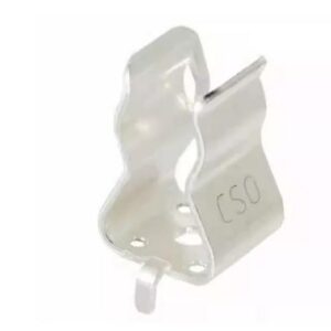
0751.0505

Schurter fuse, 0751.0505

Brand: schurter

Package: See datasheet

IN STOCK: 6768pcs

Cargo cycle: 3-7 Days

The minimum order is 1

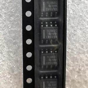
TL062CDR

Low-power JFET-input dual op-amp, 1MHz GBW, 30pA Ibias, SOIC-8, ±3.5V to ±18V

Brand: TI

Package: SOIC-8 (3.9 x 4.9 x 1.75mm)

IN STOCK: 11576pcs

Cargo cycle: 3-7 Days

The minimum order is 1

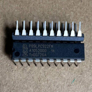
P89LPC922FN

8-bit 80C51 MCU, 8KB Flash, 256B RAM, 20-SSOP

Brand: NXP

Package: SSOP-20 (7.2 x 5.3 mm)

IN STOCK: 12628pcs

Cargo cycle: 3-7 Days

The minimum order is 1

AC0603JR-070RL

Chip Resistor, 0Ω (Zero Ohm Jumper), ±5%, 0603 (1608 Metric), 1/10W (100mW)

Brand: Yageo

Package: 0603 (1608 Metric)

IN STOCK: 100000pcs

Cargo cycle: 3-7 Days

The minimum order is 1

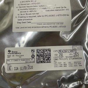
LMR34206FSC5RNXRQ1

42V 2A sync buck, 5V fixed, 2.2MHz, 18uA Iq, AEC-Q100, SOT-563

Brand: TI

Package: SOT-563 (1.6 x 1.2 x 0.55mm)

IN STOCK: 6500pcs

Cargo cycle: 3-7 Days

The minimum order is 1

AO3402

30V N-channel trench MOSFET, SOT-23, 4A, RDS(on) 52m ohm max @ 10V, Qg 10nC, 2.5V gate drive capable, -55C to +150C.

Brand: aosmd

Package: SOT-23 (2.9 x 1.6 x 1.25mm)

IN STOCK: 14066pcs

Cargo cycle: 3-7 Days

The minimum order is 1