
Opens in a new tab

SN74LS74AN

Dual D flip-flop, LS TTL, preset/clear, 25MHz, PDIP-14

6000

Effective Inventory

Image for reference only

Manufacturer Part:

SN74LS74AN

Package:

PDIP-14 (19.3 x 6.35 x 4.57mm, 2.54mm pitch, through-hole)

Brand:

Quality Commitment

Shipping & Payment

Service & Packaging

Product Manual

Description

Product Overview

The SN74LS74AN from Texas Instruments contains two independent D-type positive-edge-triggered flip-flops with complementary outputs, direct preset and clear — the TTL counterpart of the CD4013 for 5V systems in a 14-pin PDIP package.

Key Specifications

Number of Flip-Flops 2 (dual, independent)
Logic Family LS (Low-power Schottky)
Trigger Type Positive-edge (rising edge of CLK)
Supply Voltage 4.75V to 5.25V
Max Clock Frequency 25MHz typical
Preset (PRE) Active-LOW (asynchronous, sets Q=1)
Clear (CLR) Active-LOW (asynchronous, sets Q=0)
Setup Time 10ns typical
Propagation Delay 13–25ns (CLK to Q)
Operating Temperature 0°C to +70°C
Package PDIP-14 (19.3 x 6.35mm)

Features

  • Dual D-type flip-flops, positive-edge triggered
  • Asynchronous preset and clear (active-LOW)
  • Complementary outputs (Q and NOT-Q)
  • 25MHz clock frequency
  • Industry-standard 7474 pinout

Applications

  • Data register / latch
  • Frequency divider (toggle mode)
  • Switch debounce
  • Sync logic in digital systems
Product Introduction: SN74LS74AN Product Introduction

The SN74LS74AN from Texas Instruments contains two independent D-type positive-edge-triggered flip-flops with direct preset (PRE, active-LOW) and clear (CLR, active-LOW). On each rising edge of the clock, the D input is captured and appears at the Q output. The asynchronous preset (PRE=LOW) forces Q=1 regardless of CLK and D; the asynchronous clear (CLR=LOW) forces Q=0. The 7474 is the TTL counterpart of the CMOS CD4013, with active-LOW (rather than active-HIGH) preset and clear. This is the most commonly used flip-flop in TTL systems for data registers, frequency dividers, and synchronization logic. In toggle mode (NOT-Q connected to D), each flip-flop divides the clock frequency by 2. Two flip-flops in one package can divide by 4, or store 2 bits of data. The 25MHz clock frequency supports medium-speed digital systems. The A suffix denotes the improved LS version; the N suffix denotes the PDIP-14 through-hole package.

Working Principle: SN74LS74AN Working Principle

Each D flip-flop in the SN74LS74AN captures the D input on the rising edge of CLK and holds it at Q until the next rising edge. Truth table: CLK rising edge with D=0 → Q=0; D=1 → Q=1. When CLK is not rising, Q holds regardless of D. The asynchronous inputs override: PRE=LOW forces Q=1; CLR=LOW forces Q=0. Both PRE and CLR are active-LOW (unlike CD4013’s active-HIGH S and R). For normal operation, both PRE and CLR must be HIGH. If both PRE and CLR are simultaneously LOW, both Q and NOT-Q go HIGH (invalid); the final state after both are released is indeterminate. For toggle mode: NOT-Q → D; each rising clock edge toggles Q; Q frequency = CLK/2. Two 7474 flip-flops cascade: Q1 → D2, NOT-Q1 → D1, shared clock = divide-by-4. For data storage: parallel data on D1 and D2; CLK rising edge captures both bits simultaneously. The 10ns setup time means D must be stable at least 10ns before the clock edge.

Pin Description: SN74LS74AN Pin Definition and Functions
Pin Name Type Description
1 1CLR Input Flip-flop 1 clear (active LOW, sets Q=0)
2 1D Input Flip-flop 1 data input
3 1CLK Input Flip-flop 1 clock (rising edge)
4 1PRE Input Flip-flop 1 preset (active LOW, sets Q=1)
5 1Q Output Flip-flop 1 Q output
6 1NOT-Q Output Flip-flop 1 complementary output
7 GND Power Ground
8 2NOT-Q Output Flip-flop 2 complementary output
9 2Q Output Flip-flop 2 Q output
10 2PRE Input Flip-flop 2 preset (active LOW)
11 2CLK Input Flip-flop 2 clock (rising edge)
12 2D Input Flip-flop 2 data input
13 2CLR Input Flip-flop 2 clear (active LOW)
14 VCC Power Supply (5V)
Application Scenarios: In which products and applications is SN74LS74AN used
  • Toggle / Divide-by-2: 1NOT-Q → 1D; clock on 1CLK; 1Q = clock/2; 2NOT-Q → 2D; 1Q → 2CLK; 2Q = clock/4
  • 2-Bit Register: Data on 1D and 2D; shared CLK rising edge captures both bits; PRE and CLR tied HIGH for normal operation
  • Sync Logic: Asynchronous input → D1; system clock → CLK; Q1 = synchronized version of input; eliminates metastability
  • One-Shot: D tied HIGH; trigger on CLR (LOW pulse); CLK free-running; one clock-wide pulse on Q after CLR released
Alternative Models: What chips are recommended as replacements for SN74LS74AN
Model Manufacturer Key Difference Package Supply
74LS74N TI/Nexperia Original TTL version with 5V-only supply, typical propagation delay 10-15ns DIP-14 5V TTL
74LS74D TI/Nexperia Surface-mount SOIC version of LS with identical logic function SOIC-14 5V TTL
74HC74D TI/Nexperia CMOS version with wide 2-6V supply range, lower power consumption and higher noise immunity SOIC-14 2-6V CMOS
74HC74N TI/Nexperia Through-hole DIP version of HC family for prototyping and repair DIP-14 2-6V CMOS
74HCT74D TI/Nexperia CMOS with TTL-compatible input levels, ideal for mixing with LS devices at 5V SOIC-14 4.5-5.5V TTL-in
74HCT74N TI/Nexperia Through-hole DIP version of HCT family for prototyping and repair DIP-14 4.5-5.5V TTL-in
74AC74D TI/Nexperia Advanced CMOS with 2-6V supply and higher output drive current (24mA vs 6mA for HC) SOIC-14 2-6V CMOS
74AC74N TI/Nexperia Through-hole DIP version of AC family for prototyping and repair DIP-14 2-6V CMOS
74LVC74D TI/Nexperia Low-voltage CMOS for 1.65-3.6V modern logic with 24mA output drive and bus-hold inputs SOIC-14 1.65-3.6V CMOS
74LVC74N TI/Nexperia Through-hole DIP version of LVC family for prototyping and repair DIP-14 1.65-3.6V CMOS

The 7474 is a Dual D-Type Positive-Edge-Triggered Flip-Flop. Family variants span from the original LS TTL (5V only) to modern LVC/AUP (down to 0.8V). HC and HCT versions offer 2-6V CMOS operation with HCT providing TTL-compatible input thresholds for mixed 5V systems. CD4000-series equivalents offer the widest 3-18V supply range at the cost of lower switching speed. DIP packages (N suffix) are through-hole; SOIC (D suffix) and TSSOP are surface-mount.

Recommend Parts

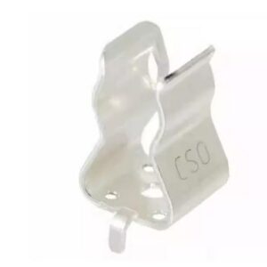
0751.0505

Schurter fuse, 0751.0505

Brand: schurter

Package: See datasheet

IN STOCK: 6768pcs

Cargo cycle: 3-7 Days

The minimum order is 1

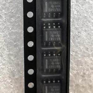
TL062CDR

Low-power JFET-input dual op-amp, 1MHz GBW, 30pA Ibias, SOIC-8, ±3.5V to ±18V

Brand: TI

Package: SOIC-8 (3.9 x 4.9 x 1.75mm)

IN STOCK: 11576pcs

Cargo cycle: 3-7 Days

The minimum order is 1

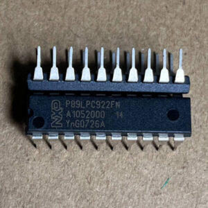
P89LPC922FN

8-bit 80C51 MCU, 8KB Flash, 256B RAM, 20-SSOP

Brand: NXP

Package: SSOP-20 (7.2 x 5.3 mm)

IN STOCK: 12628pcs

Cargo cycle: 3-7 Days

The minimum order is 1

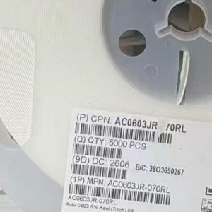
AC0603JR-070RL

Chip Resistor, 0Ω (Zero Ohm Jumper), ±5%, 0603 (1608 Metric), 1/10W (100mW)

Brand: Yageo

Package: 0603 (1608 Metric)

IN STOCK: 100000pcs

Cargo cycle: 3-7 Days

The minimum order is 1

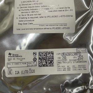
LMR34206FSC5RNXRQ1

42V 2A sync buck, 5V fixed, 2.2MHz, 18uA Iq, AEC-Q100, SOT-563

Brand: TI

Package: SOT-563 (1.6 x 1.2 x 0.55mm)

IN STOCK: 6500pcs

Cargo cycle: 3-7 Days

The minimum order is 1

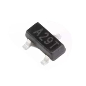
AO3402

30V N-channel trench MOSFET, SOT-23, 4A, RDS(on) 52m ohm max @ 10V, Qg 10nC, 2.5V gate drive capable, -55C to +150C.

Brand: aosmd

Package: SOT-23 (2.9 x 1.6 x 1.25mm)

IN STOCK: 14066pcs

Cargo cycle: 3-7 Days

The minimum order is 1