
Opens in a new tab

CD4014BE

8-bit parallel-in serial-out shift register, CMOS 3-18V, PDIP-16

3000

Effective Inventory

Image for reference only

Manufacturer Part:

CD4014BE

Package:

PDIP-16 (19.3 x 6.35 x 4.57mm, 2.54mm pitch, through-hole)

Brand:

Quality Commitment

Shipping & Payment

Service & Packaging

Product Manual

Description

Product Overview

The CD4014BE from Texas Instruments is an 8-stage parallel-input serial-output shift register with synchronous parallel load, ideal for reading 8 parallel data lines into a microcontroller using only 3 pins in a 16-pin PDIP package.

Key Specifications

Function 8-stage parallel-input/serial-output shift register
Technology CD4000B CMOS
Supply Voltage 3V to 18V
Parallel Inputs P1–P8 (8 lines, loaded when PAR/SER=HIGH)
Serial Input SER IN (used when PAR/SER=LOW)
Outputs Q6, Q7, Q8 (accessible outputs)
Mode Control PAR/SER (HIGH=parallel load, LOW=serial shift)
Max Clock Frequency 6MHz typical @ VDD=10V
Operating Temperature -55°C to +125°C
Package PDIP-16 (19.3 x 6.35mm)

Features

  • 8-bit parallel-to-serial conversion
  • Synchronous parallel load on clock edge
  • 3 accessible outputs: Q6, Q7, Q8
  • Cascadable for 16+ bit conversion
  • 3V-18V CMOS operation

Applications

  • Parallel-to-serial data conversion
  • GPIO expansion (8 inputs → 3 MCU pins)
  • Keyboard scanning
  • Multi-switch reading
Product Introduction: CD4014BE Product Introduction

The CD4014BE from Texas Instruments is an 8-stage static shift register with 8 parallel inputs (P1-P8) and 3 accessible outputs (Q6, Q7, Q8). On each rising clock edge, if PAR/SER=HIGH, the 8 parallel inputs are synchronously loaded into the register (P1→Q1, P2→Q2, … P8→Q8). If PAR/SER=LOW, the register shifts: each bit moves one position toward the output, and SER IN fills the vacated position. The Q8 output provides the serial data output, and Q6/Q7 provide intermediate taps. To read 8 parallel data lines into a microcontroller: (1) Set PAR/SER=HIGH and clock once to load all 8 bits. (2) Set PAR/SER=LOW and clock 8 times, reading Q8 after each clock. This uses only 3 MCU pins (CLK, PAR/SER, data from Q8) to read 8 inputs — a 5-pin saving. For 16-bit input: cascade two CD4014s by connecting Q8 of the first to SER IN of the second. The BE suffix denotes the PDIP-16 package.

Working Principle: CD4014BE Working Principle

The CD4014BE has two modes controlled by the PAR/SER input: (1) Parallel Load mode (PAR/SER=HIGH): On the rising edge of CLK, the 8 parallel inputs P1-P8 are loaded into the internal flip-flops. P1 goes to the first stage, P8 to the last (Q8). The previous serial data is overwritten. (2) Serial Shift mode (PAR/SER=LOW): On the rising edge of CLK, data shifts one position toward the output: Q1←SER IN, Q2←Q1, Q3←Q2, … Q8←Q7. The value at Q8 is the data being shifted out. To read 8 parallel inputs: first, set PAR/SER=HIGH and pulse CLK once to capture P1-P8 into the register. Then set PAR/SER=LOW and clock 8 times: on the first shift clock, Q8 (which contains P8) is available at the output pin; on the second shift clock, P7 appears; and so on until P1 is the last bit shifted out. The Q6 and Q7 outputs are useful for cascading (Q8→next SER IN) and for checking intermediate register values without additional clocking.

Pin Description: CD4014BE Pin Definition and Functions
Pin Name Type Description
1 P6 Input Parallel input 6
2 P7 Input Parallel input 7
3 P8 Input Parallel input 8
4 Q6 Output Register output stage 6
5 Q7 Output Register output stage 7
6 Q8 Output Register output stage 8 (serial output)
7 CLK Input Clock (positive edge)
8 VSS Power Ground
9 PAR/SER Input Mode: HIGH=parallel load, LOW=serial shift
10 SER IN Input Serial data input (used in shift mode)
11 P1 Input Parallel input 1 (first stage)
12 P2 Input Parallel input 2
13 P3 Input Parallel input 3
14 P4 Input Parallel input 4
15 P5 Input Parallel input 5
16 VDD Power Supply (3V to 18V)
Application Scenarios: In which products and applications is CD4014BE used
  • 8-Input GPIO Expansion: 8 switches/sensors → P1-P8; MCU: CLK, PAR/SER, Q8 → MCU; load then shift 8 times to read all 8 inputs via 3 pins
  • 16-Input Expansion: Two CD4014; Q8(#1) → SER IN(#2); shared CLK, PAR/SER; shift 16 times to read all 16 inputs via 3 MCU pins
  • Keyboard Scanner: 8 key rows → P1-P8; scan by loading and shifting; column select on separate pins
  • Parallel-to-Serial: ADC output (8-bit parallel) → P1-P8; load then shift; single wire to MCU ADC input
Alternative Models: What chips are recommended as replacements for CD4014BE
Model Manufacturer Key Difference Package Supply
CD4014BM TI SOIC-16 surface-mount version with identical logic function and 3-18V range SOIC-16 3-18V
CD4014BE TI Through-hole DIP version for prototyping and legacy board repair DIP-16 3-18V
HEF4014BT NXP Pin-compatible CMOS version with improved ESD protection and 3-15V supply SOIC-16 3-15V
MC144014BDR2G onsemi Pin-compatible equivalent with RoHS compliance and AEC-Q100 automotive option SOIC-16 3-18V
74HC165D TI/Nexperia HC CMOS version with higher speed and 2-6V supply for modern logic systems SOIC-16 2-6V
74HC165N TI/Nexperia HC CMOS through-hole version for prototyping with 2-6V supply range DIP-16 2-6V
74HCT165D Nexperia HCT version with TTL-compatible inputs for mixed 5V TTL/CMOS systems SOIC-16 4.5-5.5V

CD4014 is the CMOS 4000-series 8-stage parallel-in/serial-out shift register operating over the wide 3-18V supply range. The HEF4014 (NXP) and MC144014 (onsemi) are direct pin-compatible equivalents. For higher speed at the cost of narrower voltage range, the 74HC165 HC/HCT families offer significantly faster propagation delay and lower power consumption at 2-6V. Surface-mount versions use the BM/M suffix (SOIC); through-hole versions use the BE suffix (DIP).

Recommend Parts

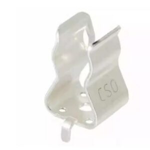
0751.0505

Schurter fuse, 0751.0505

Brand: schurter

Package: See datasheet

IN STOCK: 6768pcs

Cargo cycle: 3-7 Days

The minimum order is 1

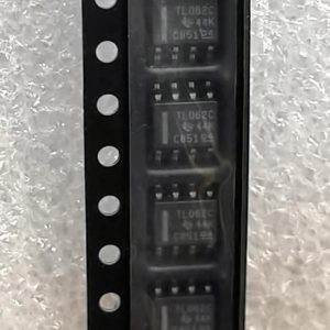
TL062CDR

Low-power JFET-input dual op-amp, 1MHz GBW, 30pA Ibias, SOIC-8, ±3.5V to ±18V

Brand: TI

Package: SOIC-8 (3.9 x 4.9 x 1.75mm)

IN STOCK: 11576pcs

Cargo cycle: 3-7 Days

The minimum order is 1

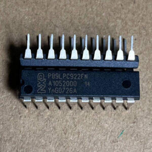
P89LPC922FN

8-bit 80C51 MCU, 8KB Flash, 256B RAM, 20-SSOP

Brand: NXP

Package: SSOP-20 (7.2 x 5.3 mm)

IN STOCK: 12628pcs

Cargo cycle: 3-7 Days

The minimum order is 1

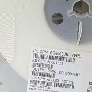
AC0603JR-070RL

Chip Resistor, 0Ω (Zero Ohm Jumper), ±5%, 0603 (1608 Metric), 1/10W (100mW)

Brand: Yageo

Package: 0603 (1608 Metric)

IN STOCK: 100000pcs

Cargo cycle: 3-7 Days

The minimum order is 1

LMR34206FSC5RNXRQ1

42V 2A sync buck, 5V fixed, 2.2MHz, 18uA Iq, AEC-Q100, SOT-563

Brand: TI

Package: SOT-563 (1.6 x 1.2 x 0.55mm)

IN STOCK: 6500pcs

Cargo cycle: 3-7 Days

The minimum order is 1

AO3402

30V N-channel trench MOSFET, SOT-23, 4A, RDS(on) 52m ohm max @ 10V, Qg 10nC, 2.5V gate drive capable, -55C to +150C.

Brand: aosmd

Package: SOT-23 (2.9 x 1.6 x 1.25mm)

IN STOCK: 14066pcs

Cargo cycle: 3-7 Days

The minimum order is 1