






Opens in a new tab

Home » Integrated Circuits ICs » AD5024BRUZ

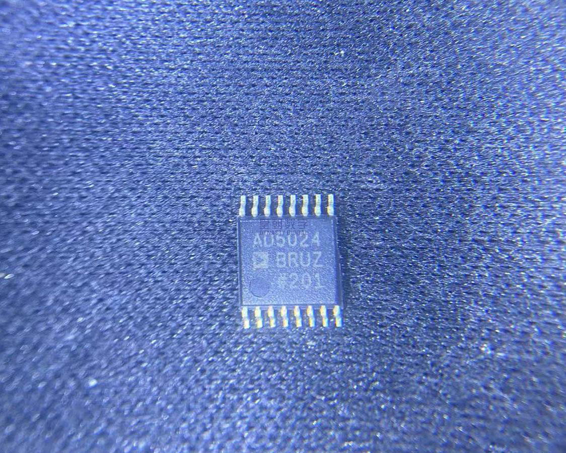
AD5024BRUZ

Quad 12-bit buffered voltage output DAC, nanoDAC, ±1 LSB INL, 4.5-5.5V supply, SPI interface up to 50MHz, rail-to-rail output, 400nA power-down, 16-TSSOP, ADI.

6780

Effective Inventory

Image for reference only

Manufacturer Part:

AD5024BRUZ

Package:

16-Lead TSSOP

Product Categories:

Quality Commitment

Shipping & Payment

Service & Packaging

Product Manual

Description

Product Overview

The AD5024BRUZ is a low-power, quad-channel 12-bit buffered voltage output DAC (digital-to-analog converter) from Analog Devices’ nanoDAC® family. Part of the AD5024/AD5044/AD5064 pin-compatible family, the AD5024 offers 12-bit resolution with ±1 LSB integral nonlinearity (INL) and differential nonlinearity (DNL) specifications, making it a fully accurate DAC suitable for precision applications. The device operates from a single 4.5V to 5.5V supply and features individual reference voltage pins for each DAC pair, providing design flexibility. A versatile 3-wire SPI-compatible serial interface operates at clock rates up to 50 MHz, compatible with standard SPI, QSPI™, MICROWIRE™, and DSP interface standards. Integrated reference buffers and output amplifiers simplify system design by eliminating the need for external buffering. The AD5024BRUZ incorporates a power-on reset circuit ensuring outputs power up to zero scale or midscale, three power-down modes reducing current consumption to typically 400 nA at 5V, hardware LDAC with software override, a CLR function with programmable clear code, and an SDO output for daisy-chaining multiple devices. Packaged in a 16-lead TSSOP and specified over the -40°C to +125°C industrial temperature range, the AD5024BRUZ is ideal for process control, data acquisition systems, portable battery-powered instruments, digital gain and offset adjustment, programmable voltage/current sources, and programmable attenuators.

Key Specifications

Parameter Value
Resolution 12 bits
Number of Channels 4 (Quad)
Architecture Voltage Output DAC with Output Buffer (nanoDAC®)
Integral Nonlinearity (INL) ±1 LSB (max)
Differential Nonlinearity (DNL) ±1 LSB (max)
Supply Voltage Range 4.5 V to 5.5 V (single supply)
Reference Pins Individual reference pins per DAC pair (VREFA, VREFB, VREFC, VREFD)
Output Type Buffered voltage output, rail-to-rail
Output Swing 0 V to VREF (rail-to-rail operation)
Interface 3-wire serial (SPI, QSPI, MICROWIRE, DSP compatible)
Maximum Serial Clock 50 MHz
Settling Time 10 µs typ to 1/2 LSB (full-scale step)
Digital Glitch Impulse 2 nV-s (typ)
DC Power-On Glitch Very low glitch at power-up
Quiescent Current 360 µA (typ) @ 5V; 480 µA (max)
Power-Down Current 400 nA (typ) @ 5V in power-down mode
Power-Down Modes 3 modes: 1kΩ to GND, 100kΩ to GND, high impedance
Power-On Reset Zero scale or midscale (selectable via POR pin)
LDAC Function Hardware LDAC pin with software LDAC override
CLR Function Asynchronous clear to programmable code
Daisy-Chain SDO pin supports multiple devices in series
Operating Temperature -40°C to +125°C
Package 16-Lead TSSOP (RU-16)
Total Unadjusted Error (TUE) < 2 mV

Features

  • Quad 12-bit buffered voltage output DAC in compact 16-lead TSSOP
  • ±1 LSB INL and DNL for high accuracy applications
  • Pin-compatible upgrade to AD5666 with better performance
  • Individual reference pins per DAC pair for flexibility
  • Rail-to-rail output operation with integrated output amplifier
  • Single 4.5V to 5.5V power supply
  • Power-on reset to zero scale or midscale (selectable)
  • 3 power-down modes plus per-channel power-down capability
  • Hardware LDAC with software LDAC override function
  • CLR function that clears to programmable DAC code
  • SDO output for daisy-chaining multiple devices
  • High-speed serial interface up to 50 MHz
  • Schmitt trigger inputs for noise immunity
  • Internal reference buffer on all reference inputs
  • Very low glitch on power-up and code transitions
  • Total unadjusted error (TUE) less than 2 mV
  • Specified over -40°C to +125°C industrial temperature range

Applications

  • Process control and industrial automation
  • Data acquisition systems and instruments
  • Portable battery-powered test and measurement equipment
  • Digital gain and offset voltage adjustment
  • Programmable voltage and current sources
  • Programmable attenuators and filters
  • Sensor calibration and trimming
  • Motor control bias and reference generation
  • Optical module bias control
  • Automotive electronics
Product Introduction: AD5024BRUZ Product Introduction

The AD5024BRUZ is a high-precision, quad-channel 12-bit digital-to-analog converter from Analog Devices’ nanoDAC® product family. Designed for applications requiring high accuracy and low power in a compact form factor, this device offers ±1 LSB integral nonlinearity (INL) and ±1 LSB differential nonlinearity (DNL) specifications, delivering fully accurate 12-bit performance across all four channels. Each channel features an integrated output buffer amplifier with rail-to-rail operation, eliminating the need for external operational amplifiers. The AD5024 operates from a single 4.5V to 5.5V supply and includes internal reference buffers for all reference pins. The device provides individual reference voltage pins for each DAC pair (VREFA for DAC A, VREFB for DAC B, etc.), giving designers flexibility to use different reference voltages on different channels. The versatile 3-wire serial interface operates at clock speeds up to 50 MHz and is compatible with SPI, QSPI, MICROWIRE, and DSP interface standards, enabling easy integration into a wide range of digital systems. An SDO output pin supports daisy-chaining multiple DACs on a single serial bus for systems requiring many output channels. Comprehensive control features include a hardware LDAC (Load DAC) pin that can be used to simultaneously update all DAC outputs, with a software LDAC override function for per-channel update control. An asynchronous CLR input clears all DAC outputs to a programmable code. The AD5024 incorporates a power-on reset circuit that ensures all DAC outputs power up to a known state (either zero scale or midscale, selected via the POR pin), preventing glitches or unexpected outputs during power-up. Three software-selectable power-down modes allow each channel to be independently placed in a low-power state with output pulled to ground through a 1kΩ or 100kΩ resistor, or set to high-impedance. In power-down mode, the typical supply current drops to just 400 nA at 5V, making the device well-suited for battery-powered applications. Total unadjusted error (TUE) is specified at less than 2 mV, ensuring excellent DC accuracy. The AD5024BRUZ is packaged in a space-saving 16-lead TSSOP package and is fully specified over the industrial temperature range of -40°C to +125°C. As part of the pin-compatible AD5024/AD5044/AD5064 family (12/14/16-bit respectively), the AD5024BRUZ provides an upgrade path for existing AD5666 designs.

Working Principle: AD5024BRUZ Working Principle

The AD5024BRUZ is a four-channel 12-bit digital-to-analog converter based on a resistor string (R-string) DAC architecture with integrated output buffer amplifiers. Each DAC channel consists of a 12-bit input register, a DAC register, and an R-string DAC followed by a rail-to-rail output buffer amplifier. The R-string architecture provides inherent monotonicity (the output always increases with increasing digital code) and very low glitch energy, which is important for applications where code transition glitches could cause problems. The digital input data is loaded through the 3-wire SPI-compatible serial interface. Each 32-bit write sequence includes 8 command bits, 4 address bits, and 12 data bits (for the 12-bit AD5024), along with additional don’t care bits for the lower resolutions. The command bits determine the operation (write to input register, update DAC register, write and update, power-down, etc.), and the address bits select which DAC channel or channels are affected. The double-buffered architecture (input register and DAC register) allows new data to be preloaded into the input registers while the DAC outputs maintain their current values. When the LDAC signal is asserted (either via hardware pin or software command), all DAC registers are simultaneously updated from their respective input registers, providing synchronized output updates across all channels. Alternatively, each channel can be updated individually by writing directly to both registers in a single write operation. The reference voltage is applied to dedicated VREF pins, with internal reference buffers ensuring high input impedance and isolating the reference from internal switching transients. The output buffer amplifiers provide rail-to-rail output swing, meaning the output voltage can approach both ground and the reference voltage, maximizing the usable output range. Power-on reset circuitry ensures all DAC registers and outputs initialize to a known state (zero scale or midscale) when power is first applied, preventing unexpected output voltages during system startup. The power-down feature reduces supply current to nanoamp levels by turning off the output buffer and placing the output in a high-impedance state or connecting it to ground through a resistor. The CLR function asynchronously clears all DAC outputs to a user-programmable value stored in the clear code register, providing a quick reset to a predefined level.

Pin Description: AD5024BRUZ Pin Definition and Functions
Pin No. Name Description
1 LDAC Load DAC input – active LOW; asynchronous update of DAC registers from input registers; can be tied LOW for synchronous update on write
2 SYNC Frame synchronization input – active LOW control input for serial interface; falling edge initiates data transfer
3 VDD Power supply – 4.5V to 5.5V; decouple with 10µF + 0.1µF to GND
4 VREFB DAC B reference voltage input – reference for DAC B channel; internally buffered
5 VREFA DAC A reference voltage input – reference for DAC A channel; internally buffered
6 VOUTA DAC A analog output – buffered voltage output from DAC channel A; rail-to-rail
7 VOUTC DAC C analog output – buffered voltage output from DAC channel C; rail-to-rail
8 POR Power-on reset select – tie to GND for zero-scale reset; tie to VDD for midscale reset
9 VREFC DAC C reference voltage input – reference for DAC C channel; internally buffered
10 CLR Clear input – asynchronous active LOW; sets all DAC outputs to programmable clear code
11 SDO Serial data output – for daisy-chaining multiple devices; data clocked out on SCLK rising edge
12 VREFD DAC D reference voltage input – reference for DAC D channel; internally buffered
13 VOUTD DAC D analog output – buffered voltage output from DAC channel D; rail-to-rail
14 VOUTB DAC B analog output – buffered voltage output from DAC channel B; rail-to-rail
15 DIN Serial data input – serial data loaded on SCLK falling edges; Schmitt trigger input
16 SCLK Serial clock input – clock for serial interface; up to 50 MHz; data latched on falling edge
GND GND Ground – exposed pad on TSSOP should connect to ground plane
Application Scenarios: In which products and applications is AD5024BRUZ used
  • Process control loop output and setpoint generation
  • Data acquisition systems and automatic test equipment (ATE)
  • Portable battery-powered instruments and measurement devices
  • Digital gain, offset, and bias voltage adjustment in signal chains
  • Programmable voltage and current source designs
  • Programmable attenuators and variable gain amplifier control
  • Sensor calibration and precision trimming applications
  • Motor control bias generation and reference programming
  • Optical transceiver module bias control and calibration
  • Automotive sensor and actuator control circuits
  • Industrial PLC analog output modules
Alternative Models: What chips are recommended as replacements for AD5024BRUZ
Model Manufacturer Key Difference
AD5044BRUZ Analog Devices 14-bit version, same package and pinout, higher resolution
AD5064BRUZ Analog Devices 16-bit version, same package and pinout, highest resolution in family
AD5624R Analog Devices 12-bit quad DAC with integrated 2.5V reference, nanoDAC+
DAC7554 Texas Instruments 12-bit quad VOUT DAC, similar specs, TI alternative
LTC2604 ADI / Linear 16-bit quad DAC with integrated reference, higher performance

Recommend Parts

ISO1176TDWR

Isolated RS-485 transceiver, 40Mbps, integrated transformer driver, SOIC-16

Brand: TI

Package: SOIC-16 (DW, wide-body, 10.3 x 10.3 mm)

IN STOCK: 6874pcs

Cargo cycle: 3-7 Days

The minimum order is 1

IRFB4020PBF

200V N-Channel HEXFET Power MOSFET, 31A, 68 mΩ RDS(on), TO-220AB

Brand: infineon

Package: TO-220AB

IN STOCK: 14149pcs

Cargo cycle: 3-7 Days

The minimum order is 1

NRF52832-QFAA-T

Nordic BLE SoC, ARM Cortex-M4 @ 64MHz, 64KB Flash, 32KB RAM, QFN-48

Package: See datasheet

IN STOCK: 10958pcs

Cargo cycle: 3-7 Days

The minimum order is 1

UCC28740DR

CVCC Flyback Controller, 700V startup, opto feedback, <10mW no-load, SOIC-7

Brand: TI

Package: SOIC-7 (4.9 x 3.9 x 1.75 mm)

IN STOCK: 4840pcs

Cargo cycle: 3-7 Days

The minimum order is 1

MMUN2211LT1G

NPN digital transistor, R1=10kΩ R2=10kΩ, 50V, 100mA, SOT-23-3, pre-biased BRT switch

Brand: Onsemi

Package: SOT-23-3 (TO-236, SC-59)

IN STOCK: 8500pcs

Cargo cycle: 3-7 Days

The minimum order is 1

TMS320F2810PBKA

C2000 Delfino DSP controller, 150MHz, 128KB Flash, BGA-179

Brand: TI

Package: BGA-179 (16 x 16 mm, PBK package)

IN STOCK: 3124pcs

Cargo cycle: 3-7 Days

The minimum order is 1





