






Opens in a new tab

ADP7157ARDZ

Adjustable low-noise LDO, 2.3-5.5V in, 1.2-3.3V out, 1.2A, 0.9uVrms noise, 82dB PSRR, 120mV dropout, 0.2uA shutdown, precision enable, 8-SOIC, ADI ADP71xx.

9800

Effective Inventory

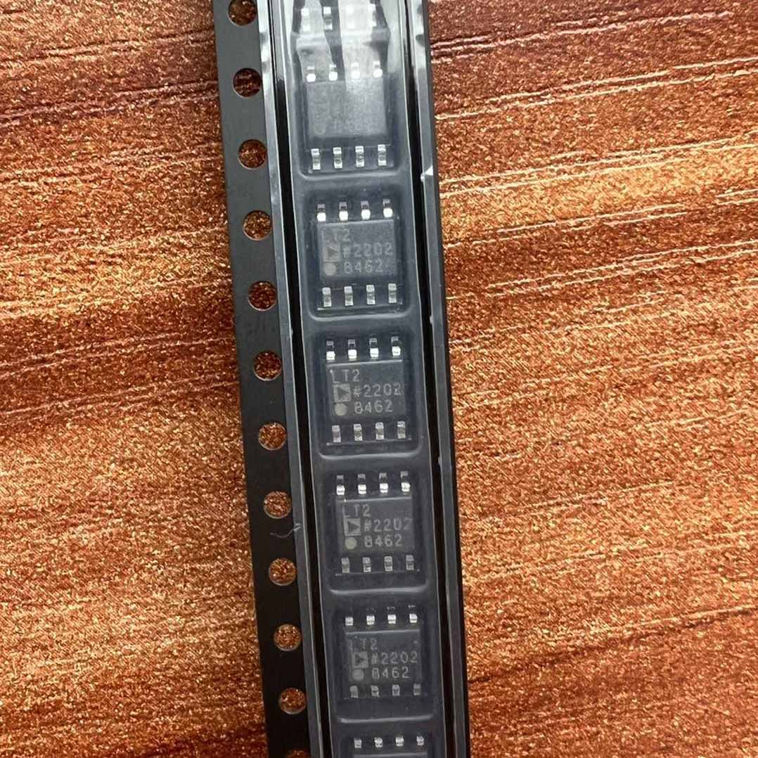
Image for reference only

Manufacturer Part:

ADP7157ARDZ

Package:

8-Lead SOIC

Quality Commitment

Shipping & Payment

Service & Packaging

Product Manual

Description

Product Overview

The ADP7157ARDZ is a high-performance adjustable low-dropout (LDO) linear regulator from Analog Devices, designed for low-noise, high power supply rejection ratio (PSRR) applications requiring up to 1.2A of output current. Operating from a 2.3V to 5.5V input supply, the device provides adjustable output voltages from 1.2V to 3.3V via an external resistor divider. Using an advanced proprietary architecture, the ADP7157 achieves exceptional PSRR of 82 dB from 1 kHz to 100 kHz and 55 dB at 1 MHz, along with ultralow output noise of only 0.9 microvolt rms from 100 Hz to 100 kHz and noise spectral density of 1.7 nV per root Hz from 10 kHz to 1 MHz. Initial accuracy is plus/minus 0.6 percent at 10 mA load, with overall accuracy over line, load, and temperature of plus/minus 1.5 percent. The dropout voltage is typically 120 mV at full 1.2A load with 3.3V output. The device is stable with only a 10 microFarad ceramic output capacitor and includes a precision enable input and shutdown mode drawing only 0.2 microamps. The ADP7157ARDZ is packaged in an 8-lead SOIC and is specified over the -40C to +125C junction temperature range.

Key Specifications

Parameter Conditions Min Typ Max Unit
Input Voltage Range (VIN) — 2.3 — 5.5 V
Adjustable Output Range — 1.2 — 3.3 V
Maximum Output Current — — — 1.2 A
Output Noise (100Hz-100kHz) BYP=1uF — 0.9 — uV rms
Output Noise (10Hz-100kHz) BYP=1uF — 1.6 — uV rms
Noise Spectral Density 10kHz to 1MHz — 1.7 — nV/root Hz
PSRR 1kHz to 100kHz — 82 — dB
PSRR at 1 MHz — — 55 — dB
Dropout Voltage IOUT=1.2A, VOUT=3.3V — 120 — mV
Initial Accuracy ILOAD=10mA, 25C -0.6 — +0.6 %
Accuracy (line, load, temp) Full range -1.5 — +1.5 %
Ground Current (IGND) 0uA load — 4.0 — mA
Ground Current (IGND) 1.2A load — 7.0 — mA
Shutdown Current EN=low — 0.2 — uA
Line Regulation VIN=2.5V to 5.5V — 0.01 — %/V
Load Regulation IOUT=0 to 1.2A — 0.05 — %
Reference Voltage (VREF) — — 1.2 — V
Output Capacitor Ceramic, for stability 10 — — uF min
Enable Input Threshold Precision enable 0.4V rising, 0.3V falling (typical) V
Junction Temperature Range Operating -40 — +125 degrees C
Thermal Shutdown Junction temperature — 150 — degrees C
Package 8-Lead SOIC (SOIC_N, R-8) —

Features

  • Input voltage range: 2.3 V to 5.5 V
  • Adjustable output: 1.2 V to 3.3 V
  • Maximum load current: 1.2 A
  • Ultralow output noise: 0.9 µV rms (100 Hz to 100 kHz)
  • Low noise spectral density: 1.7 nV/root Hz (10 kHz to 1 MHz)
  • High PSRR: 82 dB (1 kHz to 100 kHz), 55 dB at 1 MHz
  • Low dropout voltage: 120 mV typical at 1.2 A load
  • Excellent initial accuracy: ±0.6% at 10 mA
  • Total accuracy over line, load, temp: ±1.5%
  • Low ground current: 4 mA typical at no load
  • Ultralow shutdown current: 0.2 µA typical
  • Stable with 10 µF ceramic output capacitor
  • Precision enable input (accurate voltage threshold)
  • Bypass pin for additional noise reduction
  • VOUT_SENSE pin for remote sensing at load
  • Internal current limit and thermal overload protection
  • Available in 10-lead LFCSP (3x3mm) and 8-lead SOIC
  • Supported by ADIsimPower design tool
  • RoHS compliant

Applications

  • High-speed serializer/deserializer (SerDes) power
  • FPGA and processor core and I/O supply
  • Low noise RF and PLL power supplies
  • Precision analog and data acquisition circuits
  • High-speed DAC and ADC reference/analog supply
  • Medical instrumentation and patient monitoring
  • Test and measurement equipment
  • Telecommunications infrastructure
  • Industrial automation and control systems
  • Post-regulation for switching power supplies

Product Introduction: ADP7157ARDZ Product Introduction

The ADP7157ARDZ is an adjustable output low-dropout linear regulator from Analog Devices that combines high output current capability (1.2A) with ultralow noise and high power supply rejection ratio (PSRR). Designed using an advanced proprietary architecture, this LDO delivers industry-leading noise and PSRR performance while requiring only a small 10 microfarad ceramic output capacitor for stability, significantly reducing solution size and cost compared to competing high-current low-noise LDOs. The output voltage is adjustable from 1.2V to 3.3V through an external resistor divider connected to the REF_SENSE pin. The internal 1.2V bandgap reference is buffered and available on the REF pin for additional noise filtering through an external bypass capacitor, which further reduces output noise to the exceptional 0.9 microvolt rms level (100 Hz to 100 kHz). A unique VOUT_SENSE pin allows remote sensing directly at the load, compensating for voltage drops in PCB traces and ensuring accurate voltage regulation at the point of use. The precision enable input allows the device to be turned on/off with an accurately defined threshold voltage, enabling accurate power supply sequencing in multi-rail systems. The ADP7157 is available in two package options: a compact 10-lead 3x3mm LFCSP for space-constrained applications, and an 8-lead SOIC for designs preferring traditional surface-mount packages. The ADP7157ARDZ specifically is the 8-lead SOIC version. Both versions include comprehensive protection features including current limiting and thermal shutdown. With its combination of low noise, high PSRR, high current, and wide input voltage range, the ADP7157 is ideal for powering noise-sensitive circuits such as high-speed SerDes, FPGA and ASIC core supplies, RF and PLL circuits, high-speed data converters, and precision analog circuitry in test/measurement, medical, telecommunications, and industrial applications. The device is supported by ADIsimPower, ADI online power design tool that simplifies component selection and simulation.

Working Principle: ADP7157ARDZ Working Principle

The ADP7157 is a low-dropout linear regulator that uses a proprietary architecture to achieve exceptionally high PSRR and low output noise performance. At its core, the device consists of a bandgap reference, an error amplifier, a pass element (PMOS transistor), and a feedback network. The reference voltage is generated by an on-chip bandgap circuit that produces a precise 1.2V voltage with low temperature coefficient. This reference is buffered and made available on the REF pin, which can be bypassed with an external capacitor to further reduce reference noise – this is one of the key techniques that enables the ultralow noise performance of the ADP7157. The error amplifier compares the reference voltage with a divided-down sample of the output voltage and drives the gate of the PMOS pass transistor to maintain a constant output voltage. The output voltage is set by the external resistor divider connected to the REF_SENSE pin according to the formula VOUT = VREF x (R1 + R2) / R2, where R1 is the resistor from VOUT to REF_SENSE and R2 is from REF_SENSE to ground. The VOUT_SENSE pin provides Kelvin sensing capability: it is internally connected to VOUT through a small resistor and is intended to be connected directly to the load point. This eliminates the voltage drop caused by load current flowing through PCB trace resistance, ensuring that the regulated voltage is accurate at the actual point of use. The proprietary architecture of the ADP7157 provides high PSRR across a wide frequency range. At low frequencies (up to several kHz), the high DC gain of the error amplifier provides excellent line regulation and PSRR. At mid-frequencies (1 kHz to 100 kHz), the carefully designed compensation network and low-impedance pass element maintain 82 dB PSRR. At high frequencies (up to 1 MHz), the output capacitor and the low output impedance of the pass element provide 55 dB PSRR, which is significantly better than typical LDOs at these frequencies. The device also includes a precision enable circuit with an accurate voltage threshold for power sequencing, thermal shutdown protection at approximately 150C junction temperature, and current limiting to protect the pass element from overload conditions.

Pin Description: ADP7157ARDZ Pin Definition and Functions
Pin No. Name Description
1 NC No connection. Do not connect; leave floating.
2 GND Ground pin. Connect to system ground plane.
3 VOUT_SENSE Output sense pin. Internally connected to VOUT through a 10 ohm resistor. Connect as close to the load as possible for Kelvin sensing accuracy.
4 BYP Low noise bypass capacitor pin. Connect a 1 uF or greater ceramic capacitor from this pin to ground to reduce output noise.
5 EN Enable input. Drive high to turn on the regulator; drive low to turn off. For automatic startup, connect EN to VIN. Precision threshold for accurate sequencing.
6 REF_SENSE Reference sense input. This pin sets the output voltage via an external resistor divider. VOUT = VREF x (R1+R2)/R2. Connect to REF pin for fixed 1.2V output (with short).
7 REF Low noise reference voltage output (1.2V). Bypass to ground with a 1 uF or greater capacitor for noise reduction. Do not connect a load to this pin.
8 VIN Regulator input supply voltage (2.3V to 5.5V). Bypass to ground with a 10 uF ceramic capacitor near the pin.
Application Scenarios: In which products and applications is ADP7157ARDZ used
  • Powering high-speed SerDes transceivers in telecom and data center equipment
  • FPGA, ASIC, and processor core and I/O power supply rails
  • Low-noise VCO and PLL power supplies in RF and communication systems
  • High-speed ADC and DAC analog supply and reference rails
  • Precision analog front-end circuits for instrumentation
  • Medical imaging and patient monitoring equipment power
  • Test and measurement: oscilloscopes, spectrum analyzers, signal generators
  • Post-regulation after switching power supplies for noise-sensitive loads
  • Industrial control and automation signal processing circuits
  • Laboratory and scientific instrumentation
Alternative Models: What chips are recommended as replacements for ADP7157ARDZ
Model Manufacturer Key Difference
ADP7157ACPZN Analog Devices Same LDO in 10-lead 3x3mm LFCSP package, smaller footprint
ADP7158ARDZ Analog Devices 1A version, similar performance, lower current, different VOUT range options
ADM7150 Analog Devices High PSRR LDO, 800mA, ultralow noise, similar application space
LT3042 ADI / Linear Tech 200mA ultra-low noise LDO, even lower noise (0.8uVrms), lower current
TPS7A4700 Texas Instruments 1A ultra-low-noise high-PSRR LDO, TI alternative for similar specs

Recommend Parts

ISO1176TDWR

Isolated RS-485 transceiver, 40Mbps, integrated transformer driver, SOIC-16

Brand: TI

Package: SOIC-16 (DW, wide-body, 10.3 x 10.3 mm)

IN STOCK: 6874pcs

Cargo cycle: 3-7 Days

The minimum order is 1

IRFB4020PBF

200V N-Channel HEXFET Power MOSFET, 31A, 68 mΩ RDS(on), TO-220AB

Brand: infineon

Package: TO-220AB

IN STOCK: 14149pcs

Cargo cycle: 3-7 Days

The minimum order is 1

NRF52832-QFAA-T

Nordic BLE SoC, ARM Cortex-M4 @ 64MHz, 64KB Flash, 32KB RAM, QFN-48

Package: See datasheet

IN STOCK: 10958pcs

Cargo cycle: 3-7 Days

The minimum order is 1

UCC28740DR

CVCC Flyback Controller, 700V startup, opto feedback, <10mW no-load, SOIC-7

Brand: TI

Package: SOIC-7 (4.9 x 3.9 x 1.75 mm)

IN STOCK: 4840pcs

Cargo cycle: 3-7 Days

The minimum order is 1

MMUN2211LT1G

NPN digital transistor, R1=10kΩ R2=10kΩ, 50V, 100mA, SOT-23-3, pre-biased BRT switch

Brand: Onsemi

Package: SOT-23-3 (TO-236, SC-59)

IN STOCK: 8500pcs

Cargo cycle: 3-7 Days

The minimum order is 1

TMS320F2810PBKA

C2000 Delfino DSP controller, 150MHz, 128KB Flash, BGA-179

Brand: TI

Package: BGA-179 (16 x 16 mm, PBK package)

IN STOCK: 3124pcs

Cargo cycle: 3-7 Days

The minimum order is 1




