






Opens in a new tab

AO9926A

Dual N-channel MOSFET, 20V VDS, 7A ID, 26mΩ RDS(on) @ 4.5V, trench tech, low gate charge 15.2nC, logic-level drive, SOIC-8, AOS AO9926A.

25000

Effective Inventory

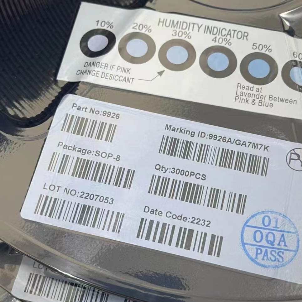
Image for reference only

Manufacturer Part:

AO9926A

Package:

SOIC-8 / SOP-8

Quality Commitment

Shipping & Payment

Service & Packaging

Product Manual

Description

Product Overview

The AO9926A is a dual N-channel enhancement mode field effect transistor (MOSFET) manufactured using advanced trench technology, providing excellent RDS(ON) performance and low gate charge. The device contains two independent N-channel MOSFETs in a single SOIC-8 package, offering a space-saving solution for applications requiring two power switches. With a drain-source voltage rating of 20V and continuous drain current of 7A per channel, the AO9926A is well-suited for battery protection, load switching, and DC-DC converter applications. The device operates over a wide gate drive range from 1.8V to 8V, making it compatible with low-voltage logic-level control signals. The two MOSFETs can be used individually, in parallel for higher current capability, or configured to form a bidirectional blocking switch. The AO9926A is commonly used in lithium-ion battery protection circuits (BMS), portable electronics power management, and motor drive applications.

Key Specifications

Parameter Conditions Min Typ Max Unit
Configuration Dual N-Channel
Drain-Source Voltage (VDS) 20 V
Gate-Source Voltage (VGS) ±8 V
Continuous Drain Current (ID) TA=25°C, VGS=4.5V 7 A
Pulsed Drain Current (IDM) 30 A
Power Dissipation (PD) TA=25°C 2 W
RDS(ON) VGS=4.5V, ID=7A, 25°C 21.6 26 mΩ
RDS(ON) VGS=4.5V, ID=7A, 125°C 29.2 36 mΩ
RDS(ON) VGS=2.5V, ID=5A 26.4 33 mΩ
RDS(ON) VGS=1.8V, ID=4A 33.3 42 mΩ
Gate Threshold Voltage (VGS(th)) VDS=VGS, ID=250μA 0.3 0.5 0.8 V
Zero-Gate Drain Current (IDSS) VDS=16V, VGS=0V 1 μA
Gate-Body Leakage (IGSS) VDS=0V, VGS=±8V 100 nA
Forward Transconductance (gFS) VDS=5V, ID=5A 22 S
Input Capacitance (Ciss) VGS=0V, VDS=10V 1050 pF
Output Capacitance (Coss) VGS=0V, VDS=10V 163 pF
Reverse Transfer Cap (Crss) VGS=0V, VDS=10V 129 pF
Total Gate Charge (Qg) VGS=4.5V, VDS=10V, ID=7A 15.2 nC
Gate-Source Charge (Qgs) 1 nC
Gate-Drain Charge (Qgd) 4 nC
Turn-On Delay (td(on)) 6.5 9 ns
Turn-Off Delay (td(off)) 56.5 ns
Body Diode VSD IS=1A 0.76 1 V
Body Diode trr 21 ns
Body Diode Qrr 7.1 nC
Junction Temperature 150 °C
Package SOIC-8 (SOP-8)

Features

  • Dual N-channel enhancement mode MOSFET
  • VDS: 20V, ID: 7A (per channel at 25°C)
  • RDS(ON): 26mΩ max @ VGS=4.5V, ID=7A
  • Low RDS(ON) at low gate voltages: 33mΩ @ 2.5V, 42mΩ @ 1.8V
  • Advanced trench technology
  • Low gate charge: 15.2nC typical
  • Wide gate drive range: 1.8V to 8V
  • Logic-level gate drive compatible
  • High cell density for low RDS(ON)
  • Two devices can be used in parallel or as bidirectional switch
  • Fast switching speed
  • Body diode with fast reverse recovery
  • SOIC-8 package
  • RoHS compliant and halogen-free

Applications

  • Lithium-ion battery protection (BMS)
  • Load switching in portable electronics
  • DC-DC converters and power management
  • Small motor drivers and motor control
  • Notebook computers and tablets
  • Smartphones and wearable devices
  • Power management ICs (PMIC) companion
  • Battery packs and chargers
  • USB power switches
  • Consumer electronics power rails
Product Introduction: AO9926A Product Introduction

The AO9926A is a dual N-channel enhancement mode MOSFET from Alpha & Omega Semiconductor, built on advanced trench technology to achieve excellent RDS(ON) with low gate charge. The device integrates two independent N-channel MOSFETs in a compact SOIC-8 package, providing a space-efficient solution for applications requiring dual power switches. With 20V VDS rating and 7A continuous drain current per channel at 25°C, the AO9926A supports a wide range of low-voltage power switching applications. The low RDS(ON) of 26mΩ maximum at VGS=4.5V ensures minimal conduction losses and high efficiency. Importantly, the device performs well even at low gate voltages — 33mΩ at 2.5V and 42mΩ at 1.8V — making it compatible with low-voltage logic control signals from microcontrollers and PMICs. The two MOSFETs can be operated independently, paralleled for higher current capability, or configured as a bidirectional blocking switch for battery protection applications. Typical applications include lithium-ion battery protection circuits (BMS), load switching in portable devices, DC-DC converters, and small motor drive circuits.

Working Principle: AO9926A Working Principle

The AO9926A contains two N-channel enhancement mode MOSFETs fabricated using trench technology. Each MOSFET operates independently and is controlled by its own gate terminal. When a positive voltage greater than the gate threshold voltage (VGS(th), typically 0.5V) is applied between the gate and source, an inversion layer forms in the channel region, allowing current to flow between drain and source. The trench architecture creates a vertical current path with high cell density, resulting in lower on-resistance and reduced gate charge compared to planar MOSFETs. The body diode of each MOSFET provides an intrinsic freewheeling path for inductive loads, with a forward voltage of approximately 0.76V and reverse recovery time of 21ns. Because both MOSFETs share the same package but have independent gate, source, and drain connections, they can be used in various configurations: independently for two separate switching functions, in parallel to double the current handling capability, or back-to-back to form a bidirectional load switch with body diode blocking.

Pin Description: AO9926A Pin Definition and Functions
Pin No. Name Description
1 S1 Source of MOSFET 1 (Channel 1)
2 G1 Gate of MOSFET 1 (Channel 1)
3 S2 Source of MOSFET 2 (Channel 2)
4 G2 Gate of MOSFET 2 (Channel 2)
5 D2 Drain of MOSFET 2 (Channel 2)
6 D2 Drain of MOSFET 2 (dual pins for current)
7 D1 Drain of MOSFET 1 (Channel 1)
8 D1 Drain of MOSFET 1 (dual pins for current)

Note: Drain pins are typically bonded together internally (pins 5-6 for D2, pins 7-8 for D1) to handle higher current and improve thermal dissipation.

Application Scenarios: In which products and applications is AO9926A used
  • Lithium-ion battery protection circuits (BMS)
  • Load switches in smartphones, tablets, notebooks
  • DC-DC converter secondary side switches
  • Small brushed DC motor drivers
  • USB power distribution and switching
  • Power path management in portable devices
  • Charger circuits and battery management
  • Consumer electronics power rails
  • Wearable devices power management
  • General purpose low-voltage switching
Alternative Models: What chips are recommended as replacements for AO9926A
Model Manufacturer Key Difference
AO9926B AOS Same series, 12V VGS rating, improved specs
AO9926C AOS Same series, different variant
Si9926CDY Vishay Compatible dual N-channel MOSFET, SOIC-8
FDS9926A onsemi Dual N-channel 20V MOSFET, SOIC-8
IRF7303 Infineon Dual N-channel MOSFET, alternative

Recommend Parts

ISO1176TDWR

Isolated RS-485 transceiver, 40Mbps, integrated transformer driver, SOIC-16

Brand: TI

Package: SOIC-16 (DW, wide-body, 10.3 x 10.3 mm)

IN STOCK: 6874pcs

Cargo cycle: 3-7 Days

The minimum order is 1

IRFB4020PBF

200V N-Channel HEXFET Power MOSFET, 31A, 68 mΩ RDS(on), TO-220AB

Brand: infineon

Package: TO-220AB

IN STOCK: 14149pcs

Cargo cycle: 3-7 Days

The minimum order is 1

NRF52832-QFAA-T

Nordic BLE SoC, ARM Cortex-M4 @ 64MHz, 64KB Flash, 32KB RAM, QFN-48

Package: See datasheet

IN STOCK: 10958pcs

Cargo cycle: 3-7 Days

The minimum order is 1

UCC28740DR

CVCC Flyback Controller, 700V startup, opto feedback, <10mW no-load, SOIC-7

Brand: TI

Package: SOIC-7 (4.9 x 3.9 x 1.75 mm)

IN STOCK: 4840pcs

Cargo cycle: 3-7 Days

The minimum order is 1

MMUN2211LT1G

NPN digital transistor, R1=10kΩ R2=10kΩ, 50V, 100mA, SOT-23-3, pre-biased BRT switch

Brand: Onsemi

Package: SOT-23-3 (TO-236, SC-59)

IN STOCK: 8500pcs

Cargo cycle: 3-7 Days

The minimum order is 1

TMS320F2810PBKA

C2000 Delfino DSP controller, 150MHz, 128KB Flash, BGA-179

Brand: TI

Package: BGA-179 (16 x 16 mm, PBK package)

IN STOCK: 3124pcs

Cargo cycle: 3-7 Days

The minimum order is 1





