






Opens in a new tab

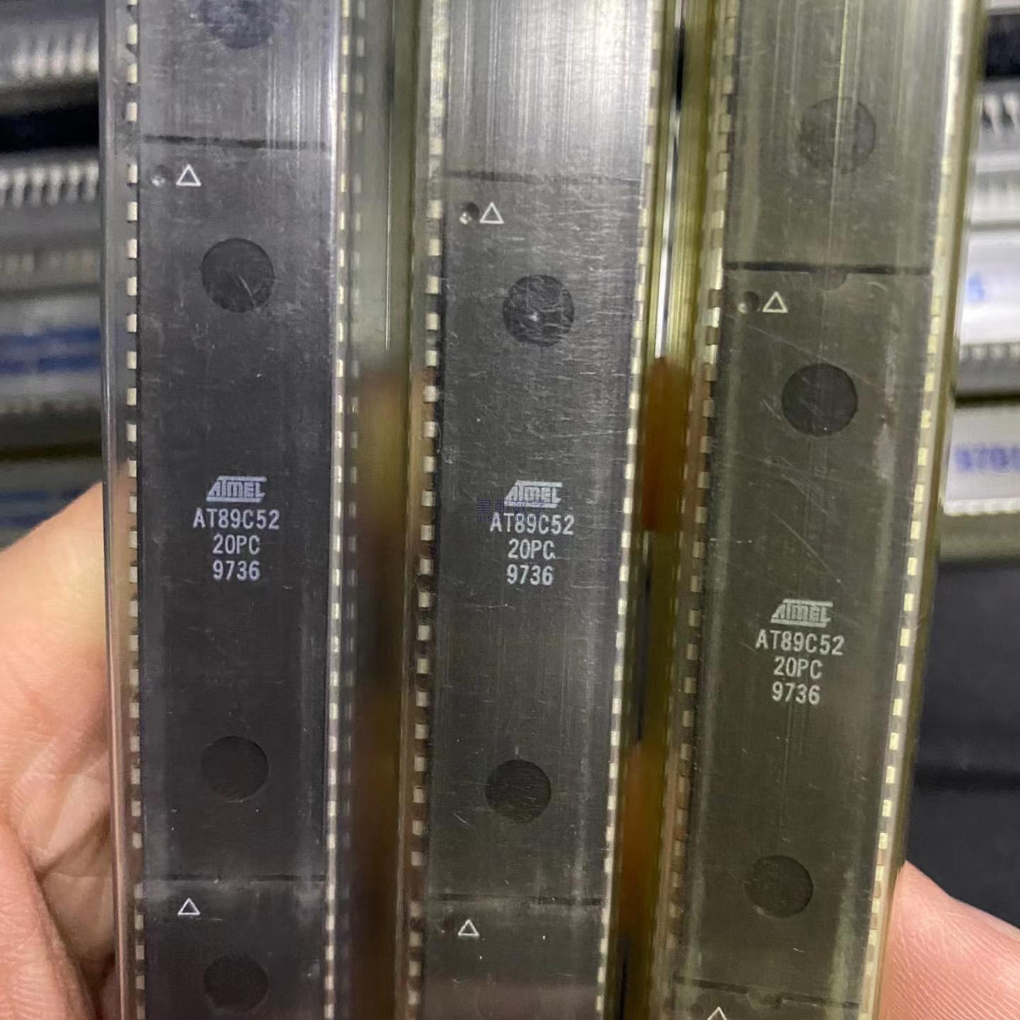
AT89C52-20PC

8-bit 8051 MCU, 8KB Flash, 256B RAM, 32 I/O, 3 timers/counters, UART, 20MHz, PDIP-40 through-hole, Atmel AT89C52-20PC, NRND use AT89S52.

8500

Effective Inventory

Image for reference only

Manufacturer Part:

AT89C52-20PC

Package:

PDIP-40 / DIP-40 (through-hole)

Quality Commitment

Shipping & Payment

Service & Packaging

Product Manual

Description

Product Overview

The AT89C52-20PC is a low-power, high-performance CMOS 8-bit microcontroller from Atmel (now Microchip), featuring 8KB of in-system programmable Flash memory and 256 bytes of internal RAM. Based on the industry-standard 80C51 architecture and instruction set, the AT89C52 is fully compatible with MCS-51 products while offering enhanced features and higher integration. The device provides three 16-bit timer/counters (compared to two in the standard 8051), 32 programmable I/O lines, a full-duplex serial UART port, and eight interrupt sources. The on-chip Flash memory can be reprogrammed in-system or via a conventional nonvolatile memory programmer, supporting 1,000 write/erase cycles. Operating at up to 20MHz (this specific -20PC speed grade), the AT89C52 delivers up to 2 MIPS of processing throughput. The device supports low-power idle and power-down modes for battery-powered applications. Packaged in a 40-pin PDIP (Plastic Dual In-line Package) with through-hole mounting, the AT89C52-20PC is widely used in education, prototyping, and cost-sensitive embedded control applications. Note: This device is not recommended for new designs; consider the AT89S52 (with ISP, watchdog timer, and dual data pointer) as a recommended replacement.

Key Specifications

Parameter Conditions Min Typ Max Unit
Core Architecture 8-bit 80C51 (MCS-51 compatible)
Operating Voltage (VCC) 4.0 5.0 5.5 V
Clock Frequency 0 Hz to max 0 20 MHz
Flash Program Memory In-System Programmable 8 KB (8192 bytes)
Flash Endurance Write/Erase cycles 1000 cycles
Internal RAM 256 x 8-bit (256 bytes)
External Memory Code + Data 64KB each (addressable)
Program Memory Lock 3-level lock bits
I/O Pins 4 ports x 8 bits 32 programmable I/O lines
Timer/Counter 0 16-bit, Mode 0/1/2/3 16-bit Timer/Counter
Timer/Counter 1 16-bit, Mode 0/1/2/3 16-bit Timer/Counter
Timer/Counter 2 16-bit, with capture 16-bit Timer/Counter (auto-reload)
Total Timers Three 16-bit timer/counters
Serial Port (UART) Full duplex 1 UART (Mode 0/1/2/3)
Interrupt Sources 8 interrupt sources, 2 priority levels
Interrupt Vectors INT0, INT1, T0, T1, Serial, T2 (6 vectors)
Oscillator External crystal / RC oscillator
Oscillator Pins XTAL1, XTAL2
Power Supply Current Active, 12MHz 25 mA
Idle Mode Current 6.5 mA
Power-down Mode Current 50 μA
Operating Temperature Commercial (PC suffix) 0 +70 °C
Package 40-pin PDIP (Plastic Dual In-line Package), through-hole
Programming Method Parallel programmer (12V VPP)
ISP Support No (parallel programming only)

Features

  • Compatible with MCS-51 (8051) instruction set and pinout
  • 8KB bytes of In-System Programmable (ISP) Flash memory
  • 1,000 write/erase cycle endurance
  • 256 x 8-bit internal RAM (double of standard 8051)
  • Three-level program memory lock (code protection)
  • 32 programmable I/O lines (Port 0, 1, 2, 3)
  • Three 16-bit timer/counters (T0, T1, T2)
  • Timer 2 with capture and auto-reload modes
  • Eight interrupt sources with two priority levels
  • Full-duplex programmable serial channel (UART)
  • Fully static operation: 0 Hz to 20 MHz
  • Low-power Idle and Power-down modes
  • On-chip oscillator and clock circuitry
  • External memory interface (64KB code + 64KB data)
  • Boolean processor (bit manipulation instructions)
  • 128 software breakpoints support
  • 40-pin PDIP package (through-hole mounting)
  • Wide industry adoption and extensive code base

Pin Configuration (PDIP-40)

Pin No. Name Description
1 P1.0 (T2) Port 1 bit 0 / Timer 2 external input
2 P1.1 (T2EX) Port 1 bit 1 / Timer 2 reload/capture
3-8 P1.2 – P1.7 Port 1 bits 2-7 (general purpose I/O)
9 RST Reset input (active high)
10 P3.0 (RXD) Port 3 bit 0 / Serial receive
11 P3.1 (TXD) Port 3 bit 1 / Serial transmit
12 P3.2 (INT0) Port 3 bit 2 / External interrupt 0
13 P3.3 (INT1) Port 3 bit 3 / External interrupt 1
14 P3.4 (T0) Port 3 bit 4 / Timer 0 input
15 P3.5 (T1) Port 3 bit 5 / Timer 1 input
16 P3.6 (WR) Port 3 bit 6 / Write strobe (external RAM)
17 P3.7 (RD) Port 3 bit 7 / Read strobe (external RAM)
18 XTAL2 Oscillator output
19 XTAL1 Oscillator input
20 GND Ground (0V)
21-28 P2.0 – P2.7 Port 2 bits 0-7 (high address byte)
29 PSEN Program Store Enable (external code read)
30 ALE/PROG Address Latch Enable / Programming pulse
31 EA/VPP External Access enable / Programming voltage
32-39 P0.0 – P0.7 Port 0 bits 0-7 (low address/data bus, open-drain)
40 VCC Supply voltage (+5V)

Applications

  • Embedded control systems
  • Industrial automation and control
  • Consumer electronics
  • Home appliances
  • Educational and learning platforms
  • Development boards and prototyping
  • Motor control and drive circuits
  • LED displays and control panels
  • Simple communication interfaces
  • Security systems
  • Toys and games
  • Legacy 8051-based system maintenance

Product Introduction: AT89C52-20PC Product Introduction

The AT89C52-20PC is a classic 8-bit microcontroller from Atmel (now Microchip Technology), built on the industry-standard 80C51 architecture. It features 8KB of in-system programmable Flash program memory, 256 bytes of internal RAM (double the capacity of the standard 8051), and three 16-bit timer/counters (T0, T1, T2) — with Timer 2 offering capture and auto-reload modes not found on the basic 8051. The device provides 32 general-purpose I/O pins organized into four 8-bit ports (P0-P3), a full-duplex UART serial port, and eight interrupt sources with two priority levels. The on-chip Flash memory supports 1,000 write/erase cycles and features three levels of program memory lock for code protection. Operating at up to 20MHz clock frequency, the AT89C52 achieves approximately 2 MIPS throughput. The device includes two power-saving modes: Idle mode stops the CPU while maintaining RAM, timers, serial port, and interrupts; Power-down mode saves RAM contents but halts the oscillator for minimal power consumption. The -20PC suffix indicates a 20MHz maximum frequency, commercial temperature range (0 to +70°C), and PDIP-40 through-hole package. This device is not recommended for new designs; AT89S52 with ISP (in-system programming), watchdog timer, and dual data pointer is the recommended successor. Despite being legacy, the AT89C52 remains extremely popular in education, prototyping, and cost-sensitive embedded applications due to its simplicity, low cost, and vast ecosystem of code examples and development tools.

Working Principle: AT89C52-20PC Working Principle

The AT89C52 is a Harvard architecture 8-bit microcontroller based on the Intel 8051 design, featuring separate program and data memory spaces. The CPU fetches instructions from Flash program memory and executes them using an 8-bit ALU, with 12 clock cycles per machine cycle (standard 8051 architecture). The 8KB Flash memory stores the user program and can be programmed via parallel programming with 12V VPP (not in-system programmable via serial — that requires AT89Sxx series). The 256 bytes of internal RAM are split: the lower 128 bytes are directly addressable for general purpose use and register banks, while the upper 128 bytes are only indirectly addressable and share addresses with Special Function Registers (SFRs). Timer/Counter 0 and 1 each support 4 modes (13-bit, 16-bit, 8-bit auto-reload, and split 8-bit), while Timer 2 adds 16-bit auto-reload and capture modes. The UART supports four modes including variable baud rate (typically driven by Timer 1 overflow). Port 0 is an 8-bit open-drain I/O port that serves as the multiplexed low address/data bus for external memory access. Port 2 provides the high address byte. Port 3 has multiple alternate functions including serial communication, external interrupts, timer inputs, and memory read/write strobes. Reset occurs when RST is held high for at least two machine cycles. The ALE signal pulses at 1/6 the oscillator frequency and is used to latch the low address byte during external memory accesses.

Pin Description: AT89C52-20PC Pin Definition and Functions
Pin No. Name Type Description
1 P1.0 / T2 I/O Port 1 bit 0 / Timer 2 external count input
2 P1.1 / T2EX I/O Port 1 bit 1 / Timer 2 reload/capture trigger
3-8 P1.2 – P1.7 I/O Port 1 bits 2 through 7 (general purpose I/O with pull-ups)
9 RST Input Reset input (active high, 2 machine cycles)
10 P3.0 / RXD I/O Port 3 bit 0 / Serial port receive
11 P3.1 / TXD I/O Port 3 bit 1 / Serial port transmit
12 P3.2 / INT0 I/O Port 3 bit 2 / External interrupt 0
13 P3.3 / INT1 I/O Port 3 bit 3 / External interrupt 1
14 P3.4 / T0 I/O Port 3 bit 4 / Timer 0 external input
15 P3.5 / T1 I/O Port 3 bit 5 / Timer 1 external input
16 P3.6 / WR I/O Port 3 bit 6 / External RAM write strobe
17 P3.7 / RD I/O Port 3 bit 7 / External RAM read strobe
18 XTAL2 Output Oscillator amplifier output (connect to crystal)
19 XTAL1 Input Oscillator amplifier input / internal clock input
20 GND Power Ground (0V)
21-28 P2.0 – P2.7 I/O Port 2 bits 0-7 / High address byte (A8-A15)
29 PSEN Output Program Store Enable (external code memory read)
30 ALE/PROG Output Address Latch Enable / Programming pulse input
31 EA/VPP Input External Access enable / Programming voltage (12V)
32-39 P0.0 – P0.7 I/O Port 0 bits 0-7 / Address/data bus (AD0-AD7), open-drain
40 VCC Power Supply voltage (+4.0V to +5.5V, typical 5V)
Application Scenarios: In which products and applications is AT89C52-20PC used
  • Industrial control and automation systems
  • Consumer electronic products
  • Home appliance control
  • Education and university 8051 courses
  • Development boards and learning platforms
  • Motor and stepper motor control
  • LED matrix and 7-segment display control
  • Security and access control systems
  • Toys, games, and hobby projects
  • Legacy system maintenance and replacement
  • Simple sensor interfacing
  • Battery chargers and power supplies
Alternative Models: What chips are recommended as replacements for AT89C52-20PC
Model Manufacturer Key Difference
AT89S52-24PU Atmel/Microchip Recommended successor – ISP, WDT, dual DPTR, 24MHz
STC89C52RC STC (宏晶) Chinese 8051 clone with ISP, similar pinout
AT89C51 Atmel 4KB Flash, 128B RAM, 2 timers (smaller version)
AT89S51 Atmel 4KB Flash, ISP, 2 timers, WDT
STC89C516RD+ STC 64KB Flash, enhanced 8051, ISP

Recommend Parts

ISO1176TDWR

Isolated RS-485 transceiver, 40Mbps, integrated transformer driver, SOIC-16

Brand: TI

Package: SOIC-16 (DW, wide-body, 10.3 x 10.3 mm)

IN STOCK: 6874pcs

Cargo cycle: 3-7 Days

The minimum order is 1

IRFB4020PBF

200V N-Channel HEXFET Power MOSFET, 31A, 68 mΩ RDS(on), TO-220AB

Brand: infineon

Package: TO-220AB

IN STOCK: 14149pcs

Cargo cycle: 3-7 Days

The minimum order is 1

NRF52832-QFAA-T

Nordic BLE SoC, ARM Cortex-M4 @ 64MHz, 64KB Flash, 32KB RAM, QFN-48

Package: See datasheet

IN STOCK: 10958pcs

Cargo cycle: 3-7 Days

The minimum order is 1

UCC28740DR

CVCC Flyback Controller, 700V startup, opto feedback, <10mW no-load, SOIC-7

Brand: TI

Package: SOIC-7 (4.9 x 3.9 x 1.75 mm)

IN STOCK: 4840pcs

Cargo cycle: 3-7 Days

The minimum order is 1

MMUN2211LT1G

NPN digital transistor, R1=10kΩ R2=10kΩ, 50V, 100mA, SOT-23-3, pre-biased BRT switch

Brand: Onsemi

Package: SOT-23-3 (TO-236, SC-59)

IN STOCK: 8500pcs

Cargo cycle: 3-7 Days

The minimum order is 1

TMS320F2810PBKA

C2000 Delfino DSP controller, 150MHz, 128KB Flash, BGA-179

Brand: TI

Package: BGA-179 (16 x 16 mm, PBK package)

IN STOCK: 3124pcs

Cargo cycle: 3-7 Days

The minimum order is 1




