






Opens in a new tab

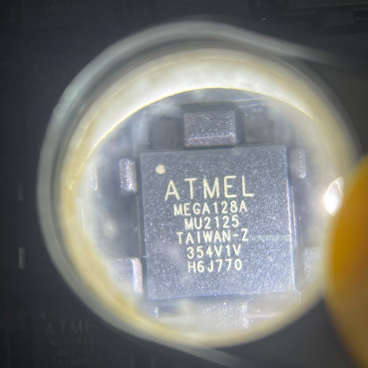
ATMEGA128A-MU

8-bit AVR MCU, 128KB Flash, 4KB SRAM, 4KB EEPROM, 53 I/O, 16MHz/16MIPS, 4 timers, 2 USARTs, 8-ch 10-bit ADC, JTAG debug, QFN-64/MLF, Atmel ATMEGA128A-MU.

4500

Effective Inventory

Image for reference only

Manufacturer Part:

ATMEGA128A-MU

Package:

QFN-64 / MLF-64 (9x9x1.0mm, 5.4mm EP)

Quality Commitment

Shipping & Payment

Service & Packaging

Product Manual

Description

Product Overview

The ATMEGA128A-MU is a high-performance, low-power CMOS 8-bit microcontroller from Atmel (now Microchip) based on the AVR enhanced RISC architecture. Featuring 128KB of in-system self-programmable Flash memory, 4KB of EEPROM, and 4KB of internal SRAM, the ATmega128A is the enhanced ‘A’ version of the classic ATmega128, offering improved electrical characteristics and wider voltage range. The device achieves a throughput of up to 16 MIPS at 16 MHz by executing powerful instructions in a single clock cycle. It provides 53 general purpose I/O lines, four flexible timer/counters with compare modes and PWM, two USARTs, a byte-oriented Two-Wire serial interface (I2C compatible), an 8-channel 10-bit A/D converter with differential input stage and programmable gain, a programmable watchdog timer, an SPI serial port, and an IEEE 1149.1 compliant JTAG test interface for on-chip debugging and programming. The ATmega128A also features six software-selectable sleep modes for power optimization. With a 2.7V to 5.5V operating voltage range and 0-16MHz speed grade, the ATmega128A is a versatile MCU suitable for a wide range of embedded applications. The -MU suffix indicates the MLF/QFN-64 surface-mount package with exposed pad (9x9mm body, 5.40mm exposed pad). This compact package provides excellent thermal performance while significantly reducing board space compared to TQFP alternatives.

Key Specifications

Parameter Conditions Min Typ Max Unit
Core Architecture 8-bit AVR RISC
Max Clock Frequency ATmega128A 0 16 MHz
Throughput @ 16MHz 16 MIPS
Total Instructions 133 instructions (most single-cycle)
Working Registers 32 x 8-bit general purpose
Multiplier 2-cycle, 8×8 → 16-bit On-chip
Flash Program Memory In-System Self-programmable 128 KB
Flash Endurance Write/Erase cycles 10000 cycles
Flash Data Retention 85°C / 25°C 20/100 years
Boot Code Section Independent lock bits Yes (optional)
Read-While-Write Yes (true RWW)
External Memory Space Optional Up to 64KB
Internal SRAM 4 KB (4096 bytes)
EEPROM Data memory 4 KB (4096 bytes)
EEPROM Endurance 100000 cycles
I/O Pins 53 programmable I/O lines
I/O Ports Ports A, B, C, D, E, F, G
8-bit Timer/Counter 0 With prescaler & compare 1 (T/C0)
8-bit Timer/Counter 2 Async capable 1 (T/C2)
16-bit Timer/Counter 1 3 compare + 1 capture 1 (T/C1, 16-bit)
16-bit Timer/Counter 3 3 compare + 1 capture 1 (T/C3, 16-bit)
Total Timers 4 timer/counters
PWM Channels Programmable resolution 2-16 bit 6 channels
8-bit PWM Channels 2 channels
USARTs Full duplex, programmable 2 USARTs (USART0, USART1)
SPI Interface Master/Slave 1 SPI
Two-Wire Interface Byte-oriented, I2C compatible 1 TWI
ADC Resolution 10-bit
ADC Channels Single-ended 8 channels
ADC Differential Channels 7 differential channels
ADC Gain Options Differential inputs 1x, 10x, 200x
Analog Comparator 1 (on-chip)
Real Time Counter Separate oscillator Yes (RTC)
Watchdog Timer On-chip oscillator Programmable WDT
JTAG Interface IEEE 1149.1 compliant Yes (boundary scan + debug + prog)
External Interrupts 8 external interrupt pins
Interrupt Levels 4-level priority
Power-On Reset Yes (POR)
Brown-out Detection Programmable Yes (BOD)
Internal RC Oscillator Calibrated Yes
ATmega103 Compatibility Mode Selected by fuse Yes
QTouch Support Capacitive touch Yes (up to 64 sense channels)
Operating Voltage ATmega128A 2.7 5.5 V
Sleep Modes 6 modes
Operating Temperature Industrial -40 +85 °C
Package 64-pad QFN/MLF (9x9x1.0mm, 5.4mm EP)

Features

  • High-performance, low-power AVR 8-bit RISC microcontroller
  • 133 powerful instructions — most single clock cycle execution
  • 32 x 8 general purpose working registers
  • Fully static operation: 0 to 16 MHz
  • Up to 16 MIPS throughput at 16 MHz
  • On-chip 2-cycle hardware multiplier (8×8 → 16-bit)
  • 128KB in-system self-programmable Flash memory
  • 10,000 Flash write/erase cycles, 20-year data retention
  • 4KB EEPROM (100,000 write cycles)
  • 4KB internal SRAM
  • Optional Boot Code section with independent lock bits
  • True Read-While-Write operation
  • Up to 64KB optional external memory space
  • Programming lock for software security
  • JTAG (IEEE std. 1149.1 compliant) interface
  • Boundary-scan capabilities
  • Extensive on-chip debug support
  • Programming of Flash, EEPROM, fuses, lock bits via JTAG
  • 53 programmable I/O lines
  • Two 8-bit Timer/Counters with separate prescalers
  • Two 16-bit Timer/Counters with compare & capture
  • Real Time Counter with separate oscillator
  • Two 8-bit PWM channels
  • 6 PWM channels with programmable resolution (2-16 bits)
  • Output Compare Modulator
  • 8-channel 10-bit ADC
  • 7 differential ADC channels with 1x/10x/200x gain
  • Byte-oriented Two-wire Serial Interface (I2C compatible)
  • Dual programmable serial USARTs
  • Master/Slave SPI serial interface
  • Programmable Watchdog Timer with on-chip oscillator
  • On-chip analog comparator
  • Power-on Reset and programmable Brown-out Detection
  • Internal calibrated RC oscillator
  • External and internal interrupt sources
  • Six sleep modes: Idle, ADC Noise Reduction, Power-save, Power-down, Standby, Extended Standby
  • Software selectable clock frequency
  • ATmega103 compatibility mode
  • Global pull-up disable
  • QTouch library support for capacitive touch
  • Wide operating voltage: 2.7V – 5.5V
  • Industrial temperature range (-40°C to +85°C)
  • 64-pad QFN/MLF package (9x9mm) with exposed pad

Applications

  • Industrial control systems
  • Motor control and drives
  • Consumer electronics
  • Home automation
  • Security systems
  • Data loggers and data acquisition
  • Medical devices
  • White goods and appliances
  • Lighting control
  • Communication systems
  • Automotive systems
  • Robotics
  • Capacitive touch interfaces
Product Introduction: ATMEGA128A-MU Product Introduction

The ATMEGA128A-MU is a high-performance 8-bit AVR RISC microcontroller from Atmel (now Microchip Technology), offering 128KB of in-system self-programmable Flash memory in a compact 64-pin QFN/MLF surface-mount package. As the ‘A’ revision of the classic ATmega128, the ATmega128A provides enhanced electrical specifications including wider operating voltage range (2.7V to 5.5V) and improved power characteristics. The AVR core executes 133 instructions — most in a single clock cycle — achieving up to 16 MIPS throughput at 16MHz. Thirty-two general purpose working registers are directly connected to the ALU for efficient operation, and an on-chip 2-cycle hardware multiplier supports fast 8×8-bit multiplication generating 16-bit results. The ATmega128A includes 4KB of SRAM and 4KB of EEPROM (with 100,000 write-cycle endurance) for non-volatile data storage. The device features 53 general purpose I/O lines multiplexed with a rich set of peripherals: four timer/counters (two 8-bit and two 16-bit) providing 6 PWM channels with programmable resolution, two full-duplex USARTs, SPI, TWI (I2C compatible), and an 8-channel 10-bit ADC. A notable ADC feature is the 7 differential input channels with programmable gain (1x, 10x, or 200x), enabling small signal measurements without external amplification. The JTAG interface provides IEEE 1149.1 boundary scan, on-chip debugging, and in-system programming of Flash, EEPROM, fuses, and lock bits. System features include Power-On Reset (POR), programmable Brown-Out Detection (BOD), internal calibrated RC oscillator, Watchdog Timer, Real-Time Counter with separate oscillator, and six sleep modes for flexible power management. The ATmega128A also supports ATmega103 compatibility mode for legacy designs and QTouch library for capacitive touch sensing. The -MU suffix indicates the MLF/QFN-64 package (9x9mm body with 5.4mm exposed pad) offering excellent thermal performance and significant board space savings compared to through-hole alternatives. This combination of performance, peripheral integration, and compact packaging makes the ATmega128A ideal for space-constrained embedded applications including industrial control, motor drives, consumer electronics, security systems, and medical devices.

Working Principle: ATMEGA128A-MU Working Principle

The ATmega128A is built on the AVR enhanced RISC architecture with Harvard architecture — separate buses for program memory and data memory. The 8-bit CPU fetches 16-bit instructions from the 128KB Flash via the program memory bus and executes them using an 8-bit ALU connected to 32 general purpose working registers. Most instructions execute in a single clock cycle, contributing to the 1 MIPS/MHz performance ratio. The Flash memory features Read-While-Write capability: the Boot Loader section (independently lockable) can run and program the Application Flash section simultaneously, enabling self-programming and firmware updates in the field. The 10-bit successive approximation ADC has 8 single-ended channels and 7 differential channels with programmable gain (1x, 10x, 200x), allowing direct measurement of small differential signals like those from strain gauges or current sensors. Two 16-bit Timer/Counters (T/C1 and T/C3) each feature three Output Compare units and one Input Capture unit, supporting PWM generation, input capture for frequency/duty measurement, and waveform generation. The Two-Wire Interface (TWI) provides I2C-compatible serial communication for connecting to sensors, EEPROMs, and other peripherals. The JTAG interface supports three major functions: boundary-scan testing per IEEE 1149.1 for PCB manufacturing test, On-chip Debug for real-time code debugging and breakpoints, and Flash/EEPROM programming. Six sleep modes provide graduated power savings: Idle (CPU stops, peripherals run), ADC Noise Reduction (CPU stops + I/O modules except ADC and async timer), Power-save (asynchronous timer runs), Power-down (full sleep, only external interrupts or reset wake), Standby (main oscillator runs + fast wake-up), and Extended Standby (both main oscillator and async timer run). The Power Reduction Register allows individual peripheral clocks to be gated off for additional energy savings.

Pin Description: ATMEGA128A-MU Pin Definition and Functions

The ATmega128A in MLF/QFN-64 package (9x9mm) has the following major pin groups (same pinout as TQFP-64, but with exposed bottom pad):

Port/Pin Group Description
Port A (PA0-PA7) 8-bit bidirectional I/O with internal pull-ups / External memory AD0-AD7
Port B (PB0-PB7) 8-bit bidirectional I/O / SPI (SS, MOSI, MISO, SCK), Timer1 PWM, OC0
Port C (PC0-PC7) 8-bit bidirectional I/O / TWI (SDA, SCL), Timer3 PWM
Port D (PD0-PD7) 8-bit bidirectional I/O / USART0, INT0-INT1, OC2, ICP1
Port E (PE0-PE7) 8-bit bidirectional I/O / USART1, INT2-INT3, OC3A
Port F (PF0-PF7) 8-bit bidirectional I/O / ADC0-ADC7, JTAG (TCK, TMS, TDO, TDI)
Port G (PG0-PG4) 5-bit bidirectional I/O / ALE, RD, WR, TOSC1, TOSC2
Power Pins VCC, AVCC, AREF, GND (multiple)
Reset RESET (active low)
Oscillator XTAL1, XTAL2
Exposed Pad Bottom center pad – must be soldered to GND

Total: 7 ports = 53 I/O pins (Port A-G with 8+8+8+8+8+8+5 = 53 pins). Bottom exposed pad should be connected to ground for thermal and electrical performance.

Application Scenarios: In which products and applications is ATMEGA128A-MU used
  • Industrial control and automation systems
  • Motor control and motor drives
  • Consumer electronics and appliances
  • Home automation and smart devices
  • Security and access control systems
  • Data acquisition and data logging
  • Medical equipment and devices
  • LED lighting control systems
  • Communication and networking equipment
  • Automotive electronics
  • Robotics and embedded control
  • Capacitive touch interfaces and keypads
Alternative Models: What chips are recommended as replacements for ATMEGA128A-MU
Model Manufacturer Key Difference
ATMEGA128A-AU Atmel Same die, TQFP-64 package instead of QFN
ATMEGA128L-8MU Atmel Low voltage version (2.7-5.5V), 8MHz max
ATMEGA1281V-8MU Atmel Enhanced version, picoPower, extended features
ATMEGA2561-16MU Atmel 256KB Flash (double), same pinout
STM32F103C8T6 STMicroelectronics Cortex-M3 alternative, 64KB Flash, LQFP-48

Recommend Parts

ISO1176TDWR

Isolated RS-485 transceiver, 40Mbps, integrated transformer driver, SOIC-16

Brand: TI

Package: SOIC-16 (DW, wide-body, 10.3 x 10.3 mm)

IN STOCK: 6874pcs

Cargo cycle: 3-7 Days

The minimum order is 1

IRFB4020PBF

200V N-Channel HEXFET Power MOSFET, 31A, 68 mΩ RDS(on), TO-220AB

Brand: infineon

Package: TO-220AB

IN STOCK: 14149pcs

Cargo cycle: 3-7 Days

The minimum order is 1

NRF52832-QFAA-T

Nordic BLE SoC, ARM Cortex-M4 @ 64MHz, 64KB Flash, 32KB RAM, QFN-48

Package: See datasheet

IN STOCK: 10958pcs

Cargo cycle: 3-7 Days

The minimum order is 1

UCC28740DR

CVCC Flyback Controller, 700V startup, opto feedback, <10mW no-load, SOIC-7

Brand: TI

Package: SOIC-7 (4.9 x 3.9 x 1.75 mm)

IN STOCK: 4840pcs

Cargo cycle: 3-7 Days

The minimum order is 1

MMUN2211LT1G

NPN digital transistor, R1=10kΩ R2=10kΩ, 50V, 100mA, SOT-23-3, pre-biased BRT switch

Brand: Onsemi

Package: SOT-23-3 (TO-236, SC-59)

IN STOCK: 8500pcs

Cargo cycle: 3-7 Days

The minimum order is 1

TMS320F2810PBKA

C2000 Delfino DSP controller, 150MHz, 128KB Flash, BGA-179

Brand: TI

Package: BGA-179 (16 x 16 mm, PBK package)

IN STOCK: 3124pcs

Cargo cycle: 3-7 Days

The minimum order is 1





