






Opens in a new tab

Home » Integrated Circuits ICs, Video ICs » EP3C40F484C8N

EP3C40F484C8N

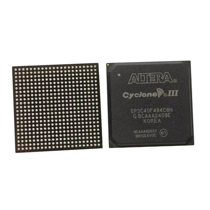
Cyclone III FPGA, 39,264 LEs, M9K RAM, 18×18 multipliers, 484-pin FBGA, C8 (commercial)

2715

Effective Inventory

Image for reference only

Manufacturer Part:

EP3C40F484C8N

Package:

484-pin FBGA

Brand:

Product Categories:

Quality Commitment

Shipping & Payment

Service & Packaging

Product Manual

Description

Product Overview

EP3C40F484C8N is an Intel/Altera Cyclone III EP3C40 FPGA, 39,264 LEs, 484-pin FBGA, commercial grade, speed grade 8.

Key Specifications

Type Cyclone III FPGA
Logic Elements 39,264 LEs
Embedded RAM 1,161,216 bits
Multipliers 252 (18×18)
Package 484-pin FBGA (F484)
Speed Grade 8
Series EP3C40

Features

  • 39K LE Cyclone III FPGA
  • 1.16M bits embedded M9K RAM
  • 252 embedded 18×18 multipliers
  • 484-pin FBGA package

Applications

Refer to manufacturer datasheet for detailed application information and design guidelines.

Product Introduction: EP3C40F484C8N Product Introduction

EP3C40F484C8N is an Intel/Altera Cyclone III EP3C40 FPGA, 39,264 LEs, 484-pin FBGA, commercial grade, speed grade 8.

Working Principle: EP3C40F484C8N Working Principle

The EP3C40F484C8N is a Cyclone III FPGA from Intel/Altera. It uses a lookup table (LUT)-based fabric with configurable logic elements (LEs) that implement combinatorial and sequential logic. Embedded M9K/M4K memory blocks provide on-chip RAM, ROM, and FIFO functions. Dedicated DSP multipliers accelerate arithmetic operations. A programmable interconnect matrix routes signals between logic, memory, and I/O elements. Configuration is loaded from external flash or via JTAG/AS programming. The device supports multiple I/O standards including LVDS, SSTL, and HSTL for interfacing with diverse external devices.

Pin Description: EP3C40F484C8N Pin Definition and Functions
Pin Group Name Description
I/O GPIO Banks Programmable I/O with multiple standard support (LVDS, SSTL, HSTL, LVCMOS)
Power VCCIO, VCCINT, VCCPLL Core, I/O, and PLL supply voltages
Ground GND Ground reference
Config DATA, DCLK, nCSO JTAG/AS/AP configuration interface
Clock CLK, PLL Dedicated clock inputs and PLL feedback
Transceiver TX/RX (if applicable) High-speed serial transceiver lanes
Application Scenarios: In which products and applications is EP3C40F484C8N used
  • Digital signal processing and filtering
  • Custom protocol implementation (UART, SPI, I2C, PCIe)
  • Video and image processing pipelines
  • Motor control and industrial automation
  • Prototyping and glue logic integration
Alternative Models: What chips are recommended as replacements for EP3C40F484C8N
Model Manufacturer Key Difference
XC7K325T Xilinx Kintex-7, 326K LE, Artix-class performance
ECP5-85 Lattice 84K LUT, low-cost mid-range alternative
iCE40HX8K Lattice 8K LUT, ultra-low-cost small form factor

Recommend Parts

ISL95855HRTZ-T

IMVP8 3+2+1 phase buck controller, R3 technology, 4.5-25V input, 48-TQFN

Brand: Renesas

Package: 48-TQFN (6×6 mm, exposed pad)

IN STOCK: 2156pcs

Cargo cycle: 3-7 Days

The minimum order is 1

IRFB4019PBF

150V N-Channel HEXFET Power MOSFET, 47A, 34 mΩ RDS(on), TO-220AB

Brand: infineon

Package: TO-220AB

IN STOCK: 2409pcs

Cargo cycle: 3-7 Days

The minimum order is 1

MSP430F247TPMR

TI MSP430 MCU, 16-bit RISC, 92KB Flash, 8KB RAM, 16MHz, LQFP-64

Package: See datasheet

IN STOCK: 13371pcs

Cargo cycle: 3-7 Days

The minimum order is 1

UCC28740DR

CVCC Flyback Controller, 700V startup, opto feedback, <10mW no-load, SOIC-7

Brand: TI

Package: SOIC-7 (4.9 x 3.9 x 1.75 mm)

IN STOCK: 4840pcs

Cargo cycle: 3-7 Days

The minimum order is 1

MMUN2211LT1G

NPN digital transistor, R1=10kΩ R2=10kΩ, 50V, 100mA, SOT-23-3, pre-biased BRT switch

Brand: Onsemi

Package: SOT-23-3 (TO-236, SC-59)

IN STOCK: 8500pcs

Cargo cycle: 3-7 Days

The minimum order is 1

PIC32MX795F512L-80I/PF

32-bit PIC32MX MCU with Ethernet/CAN/USB, 80MHz, 512KB Flash, TQFP-100, industrial

Brand: MICROCHIP

Package: TQFP-100 (14 x 14 mm)

IN STOCK: 7912pcs

Cargo cycle: 3-7 Days

The minimum order is 1




